


ZCU111 User Guide : Block Diagram, Features and Specifications
ZCU111 Evaluation Board Overview
The ZCU28DR RFSoC device from AMD is featured on the ZCU111 evaluation board. The assessment of soft decision forward error correction (SDFEC), integrated RF-DAC and RF-ADC capability, FPGA fabric, and RFSoC features—such as the dual-core Arm Cortex-R5 real-time processors and the quad-core Arm Cortex®-A53 processing system (PS)—is made possible by this board. Many common board-level capabilities required for design development are on the ZCU111 evaluation board, including networking interfaces, DDR4 memory, an FMC+ expansion connection, and access to the novel RF-FMC interface.
An FMC XM500 balun transformer add-on card is included with the ZCU111 evaluation board kit out of the box to facilitate loopback evaluation and signal processing. This card has SMAs for custom baluns and filtering in addition to onboard high-frequency and low-frequency baluns.
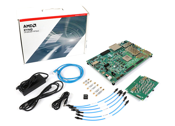
Figure1-ZCU111 Evaluation Board
ZCU111 Board Diagram
ZCU111 Evaluation Board Block Diagram
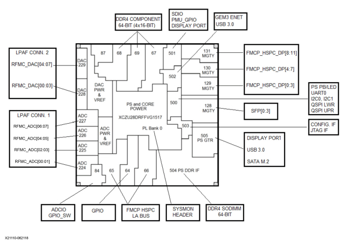
Figure2-ZCU111 Board Diagram
ZCU111 Evaluation Board Features
- XCZU28DR-2E, FFVG1517 package
- Form factor: rectangular 11.811 in. x 7.874 in. x 0.1 in.
- Configuration from:
° Dual Quad SPI
° Micro SD card
° USB-to-JTAG bridge
- Clocks
° GTR_REF_CLK_DP 27 MHz
° GTR_REF_CLK_USB3 26 MHz
° GTR_REF_CLK_SATA 125 MHz
° CLK_100 100 MHz
° CLK_125 125 MHz
° PS_REF_CLK 33.33 MHz
° USER_MGT_SI570 (default 156.25 MHz)
° USER_SI570 (default 300 MHz)
- PS DDR4 4 GB 64-bit SODIMM
- PL DDR4 4 GB 64-bit component (4x16-bit)
- PS GTR (bank 505) assignment
° DisplayPort 1.2 transmits only (two GTR)
° USB3 (one GTR)
° SATA with M2 connector (one GTR)
- PL GTY assignment (16 total)
° SFP28 (four, bank GTY128)
° FMCP HSCP DP (four, bank GTY129)
° FMCP HSCP DP (four, bank GTY130)
° FMCP HSCP DP (four, bank GTY131)
- PL FMCP HSCP (FMC+) connectivity - full LA[00:33] bus
- PS MIO connectivity
° PS MIO[0:5, 7:12]: dual Quad SPI flash memory
° PS MIO[13]: PS_GPIO2
° PS MIO[14:17]: two channels of I2C
° PS MIO[18:19]: UART (one of three FT4232 UART channels)
° PS MIO[22:23]: PS_PB, PS_LED I/F
° PS MIO[26]: platform management unit (PMU)
° PS MIO[27:30]: DisplayPort control
° PS MIO[32:37]: PMU_GPIO[0:5]
° PS MIO[38]: PS_GPIO1
° PS MIO[44:51]: SD I/F
° PS MIO[52:63]: USB3.0
° PS MIO[64:77]: GEM3 Ethernet
- PL I/O connections:
° PL-side user DIP switch (8-position)
° PL-side CPU reset pushbutton
° PL-side user LEDs (eight)
° PL-side user pushbuttons (five, geographic N, S, E, W, C)
° PL-side PMOD0/1 (two R.A. 2x6 receptacles)
- Security - PSBATT button battery backup
- SYSMON header
- Operational switches (power on/off, PROG_B, boot mode DIP switch)
- Operational status LEDs (INIT, DONE, PS STATUS, PGOOD)
- Power management
- System controller (MSP430)
ZCU111 Board Specifications
|
Board Specifications |
Value |
|
Height |
11.811 inch (30.0 cm) |
|
Width |
7.874 inch (20.0 cm) |
|
Thickness (+/-5%) |
0.10799 inches (0.2743 cm) |
|
Operating Environmental Temperature |
0◦C to +45◦C |
|
Storage Environmental Temperature |
-25◦C to +60◦C |
|
RF Data Converter |
|
|
# of 12-bit ADCs |
8 |
|
Max Rate (GSPS) |
4.096 |
|
# of 14-bit DACs |
8 |
|
Max Rate (GSPS) |
6.554 |
|
SD-FEC |
8 |
|
Memory |
|
|
PS DDR4 |
4GB 64-bit SODIMM |
|
SD-Card |
Yes |
|
M.2 SATA Connector |
Yes |
|
QSPI |
2 |
|
Communications & Networking |
|
|
USB UART/JTAG |
1 |
|
RJ45 |
1 |
|
SFP+ |
4 |
|
USB 3.0 |
1 |
|
Display |
|
|
DIP Switches |
Yes |
|
LEDs |
Yes |
|
Push Buttons |
Yes |
|
VESA DisplayPort 1.2 |
Yes |
|
Expansion Connectors |
|
|
FMC-HPC Connector |
2 |
|
PMOD |
2 |
|
RFMC 1.0 |
2 |
|
Add-on Cards |
|
|
XM500 |
Yes |
|
Control & I/O |
|
|
I2C |
Yes |
|
PMBUS |
Yes |
|
JTAG PC4 Header |
Yes |
|
Boot Options |
|
|
SD Boot |
Yes |
|
QSPI Boot |
Yes |
|
JTAG Boot |
Yes |
|
Power |
|
|
12V Wall Adapter |
Yes |
|
ATX Power Compatible |
Yes |
ZCU111 Benefits
- Evaluation Board ZCU111 for Zynq UltraScale+ RFSoC with XCZU28DR-2FFVG1517E RFSoC
- A 4GB, 64-bit DDR4 component connected to a programmable logic (PL) system
- 4GB 64-bit DDR4 SODIMM, 2400MT/s, connected to Processor Subsystem (PS)
- The SFP28 cage has been gated to accommodate up to 4 SFP/SFP+/zSFP+/SFP28 modules.
- USB3, DisplayPort, and SATA
- 34 user-defined differential I/O signals and 12 33Gb/s GTY transceivers are included in the FPGA Mezzanine Card (FMC+) interface for I/O expansion.
- Add-on card for XM500 RFMC balun transformer featuring 4 DACs/4 ADCs to baluns 4 ADCs and 4 DACs to SMAs
ZCU111 Evaluation Board
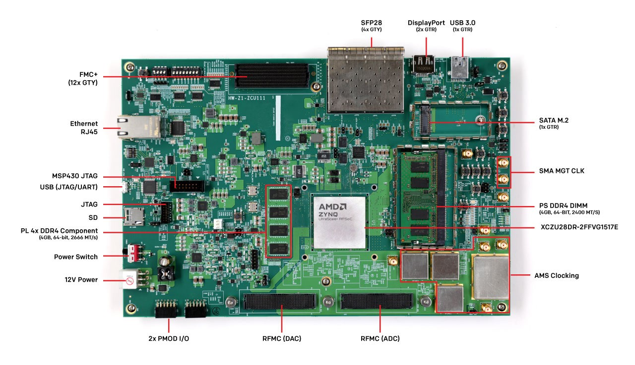
Figure3-ZCU111
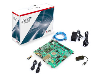
What's Inside the Box?
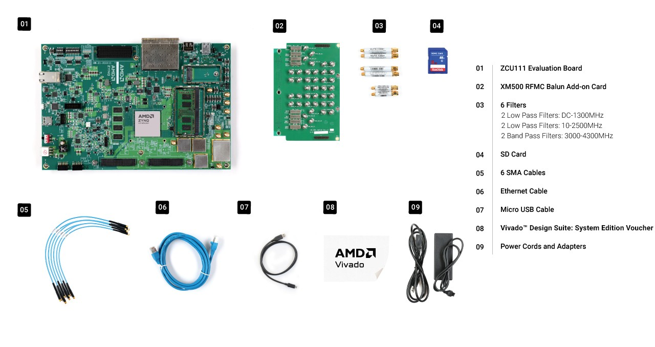
Figure 4- What's Inside the Box?
 ZCU106 Evaluation Kit: Overview, Features,Components, Quick start guide5/10/2024 2
The ZCU106 Evaluation Kit is a development board designed by Xilinx for prototyping and evaluating designs based on their Zynq UltraScale+ MPSoC platform. This guide will provide an overview of the kit, its components, and how to get started with it.
Read More > Infineon's profit decreases, memory Q2 contract price increase revised upwards5/9/2024 11
Infineon recently announced its results for the second quarter of fiscal year 2024. Revenue was 3.632 billion euros, down 12% year-on-year and 2% month-on-month; profit was 707 million euros, down 40% year-on-year and 15% month-on-month; gross profit margin was 38.6%. , a year-on-year decrease of 8 percentage points and a month-on-month decrease of 4.6 percentage points.
Read More > NXP and ON Semiconductor released financial reports5/5/2024 26
NXP and ON Semiconductor released financial reports, rising copper prices were transmitted to the IC industry
Read More > Tesla cuts 10% of global layoffs, Samsung increases NAND flash memory production this quarter4/17/2024 28
1.Tesla announced 10% of its global layoffs, with a higher domestic proportion
Read More > How much do you know about fpga design engineer?4/16/2024 54
Circuitry can be a complex field. The circuit must be completely redone because even the smallest error can drastically alter the project's outcome. One of the numerous individuals involved in circuit building is the FPGA design engineer.An electrical engineer with a focus on designing Field Programmable Gate Array integrated circuits is known as an FPGA engineer.After reading this site, you will be fully informed about fpga design engineers.
Read More >
Hot News
- Diode Overview: Application in Automotive Alternator Rectifiers
- Ultra-low power consumption of STM32U575/585 microcontrollers(MCU)
- The Best Guide to Transistor
- Basic Information about Temperature Sensor
- Voltage-Controlled Oscillator: Principle, Type Selection, and Application
- Electronic Component Symbols: Resistor, Capacitor, Transformers and Connectors
SUPPORT
ABOUT BITFOIC
QUICK LINKS
Connect with us
Tel: 86-755-23606554
E-mail: [email protected]
Address: Room A29, 24 / F, Hoi Tak Wai, Prince Edward industrial building, 706 Prince Edward Road East, San Po Kong, Kowloon,Hongkong
Mon-Fri: 09.30 AM - 18.30 PM


