


Ultra-low power consumption of STM32U575/585 microcontrollers(MCU)
Introduction
The STM32U5 series offers low-power advanced microcontrollers based on the Arm® Cortex®-M33 core to meet the demanding power and performance requirements of smart applications, including wearable devices, personal medical devices, home automation, and industrial sensors.
The STM32U5 microcontroller series has built-in up to 2MB of flash memory (dual BANK architecture) and 786 KB of SRAM, helping to improve performance to a new level.
The STM32U5 has 8 package options (48~169 pins) and a large number of product numbers, and also supports operation at ambient temperatures up to 125°C.
Catalog
ⅠSTM32U575/585 Overview
Ⅱ High-efficiency processing
2.1 Internal Regulator Efficiency
2.2 ICACHE Efficiency
2.3 Flash Efficiency
Ⅲ STM32U575/585 Ultra-low Power Consumption Characteristics
3.1 Low Power Mode
3.1.1 Sleep Mode
3.1.2 Shutdown Mode
3.1.3 Standby Mode
3.1.4 Shutdown Mode
3.2 Power consumption optimization
3.2.1 ICACHE IN RUN MODE
3.2.2 Flash in run and sleep mode
3.2.3 Power Control Optimization
3.2.4 RCC in Low Power Mode
3.2.5 I/O states in low-power modes
3.2.6 Internal SRAM
3.2.7 Peripheral Clock Gating in Run and Stop Modes
3.3 Optimizing Peripheral Power Consumption Using LPBAM
3.3.1 Peripherals supporting LPBAM
3.3.2 Main Examples
Ⅳ Selection Method of Low Power Consumption Mode
4.1 PROCESS
4.2 INACTIVE
4.3 Sleep mode selection
4.4 Low Power Mode Selection
4.5 Impact of conversion
Ⅴ Conclusion
ⅠSTM32U575/585 Overview
The STM32U575/585 microcontrollers (MCUs) are based on the high-performance Arm® 32-bit Cortex® M33 CPU with Arm® TrustZone® and FPU. Manufactured with a novel architecture, these MCUs achieve best-in-class ultra-low power performance thanks to their high flexibility and advanced peripheral set. The STM32U575/585 devices enable applications to achieve very high energy efficiency.
STM32U575/585 devices with a "Q" suffix (e.g. STM32U5xxxxQ) support the use of the internal SMPS in run and low-power modes, enabling the design of very efficient low-power applications
With an integrated ART accelerator 8 KB instruction cache, the STM32U575/585 MCUs can operate at frequencies up to 160MHz, achieving 240 DMIPS performance while maintaining extremely low dynamic power consumption.
The STM32U575/585 devices embed a large number of intelligent high-performance peripherals with various advanced ultra-low-power analog functions. With LPBAM (Low Power Background Autonomous Mode), many peripherals including communications, analog, timers, and audio are functional and autonomously enter shutdown mode with direct memory access. The combination of ultra-low power design and processing performance enables these devices to achieve industry-leading EEMBC® ULPBench™ scores of up to 535 ULPMark™.
The STM32U575/585 MCUs incorporate a variety of innovations that minimize power consumption in different modes while retaining most of the existing peripherals and are well pin-compatible, enabling easy migration from existing products transplant.
Thanks to its built-in internal voltage regulator and voltage regulation, consumption in active mode are kept as low as possible, regardless of the external supply voltage. This makes these devices ideal for battery-powered products requiring supply voltages as low as 1.71 V.
Additionally, they feature multiple voltage domains, allowing products to be powered at low voltages, while the analog-to-digital and digital-to-analog converters can operate from high supply and reference voltages up to 3.6V.
The STM32U575/585 devices can support a battery backup domain to keep the RTC (Real Time Clock) running and can support a bank of 32 registers (32 bits wide each) that retain their contents when power is lost. This optional backup battery can be charged while the main power is available.
These devices support several main low-power modes, each of which has multiple sub-mode options. This allows designers to achieve an optimal compromise between low-power performance, short startup times, the set of available peripherals, and the maximum number of wake-up sources.
Ⅱ High-efficiency processing
High processing performance (expressed in DMIPS/MHz) is achieved in run mode due to the use of the Cortex M33 core associated with its memory interface. To ensure high-performance operation at the maximum operating frequency, the STM32U575/585 devices embed the ART accelerator instruction cache (cache), which shields the Flash access wait state. 1.5 DMIPS/MHz processing performance regardless of system clock frequency.
The STM32U575/585 devices support dynamic voltage scaling in order to optimize their power consumption in Run mode. The voltage provided by the main voltage regulator powering the logic (VCORE) can be adjusted according to the highest operating frequency of the system. For more details, please refer to the reference document [1]
The main regulator operates within the following ranges:
- Range 1 (V core = 1.2 V) with CPU and peripherals running up to 160 MHz
- Range 2 (V core = 1.1 V) with CPU and peripherals running up to 110 MHz
- Range 3 (V core = 1.0 V) with CPU and peripherals running up to 55 MHz
- Range 4 (V core = 0.9 V) with CPU and peripherals running up to 25 MHz
Unless otherwise stated, all power consumption figures used in this application note are based on typical specifications at TA = 25 °C and VDD = 3.0 V extracted from reference [2].
Notes:
When using the low-power regulator, the system clock can be MSIS up to 24MHz (default 4MHz) or HSI16, depending on the software configuration.
2.1 Internal Regulator Efficiency
The STM32U575/585 devices embed two internal voltage regulators, which can be selected at runtime according to the application requirements:
- SMPS Buck Converter
- Linear Voltage Regulators (LDOs)
LDO and SMPS regulators have two modes:
- Main regulator (used when performance is required)
- Low power regulator
Both voltage regulators can provide four different voltages (voltage regulation), while also operating in shutdown mode.
|
Regulator mode |
Device mode |
|
main regulator(Range1 2 3 4) |
operation、sleep、shutdown |
|
Low Power Regulators |
shutdown1、shutdown2、shutdown3(Standby for 8KB or full SRAM2) |
The figure below shows the typical current consumption (as a function of system frequency) of the STM32U575/585 microcontrollers in run mode for SMPS and LDO configurations.
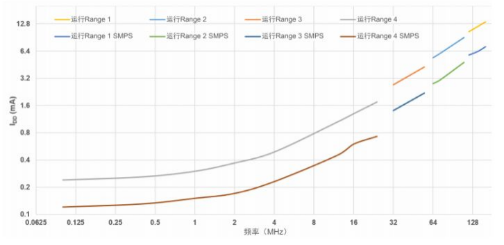
Figure 1. SMPS vs. LDO current consumption when running with ICACHE on, single-way, and prefetch enabled
The lowest power consumption is achieved when running from internal Flash with a single-way cache. Instruction caches tend to reduce the number of accesses to memory, which reduces overall current consumption. When using ICACHE, the current consumption of internal SRAM is similar to Flash.
The graph below shows this curve translated to power efficiency at CPU frequency (divide it by current draw and multiply by supply voltage to get a power graph).
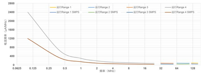
Figure 2. The power efficiency of SMPS vs. LDO in the running mode with ICACHE enabled, single-leave, and prefetch enabled
2.2 ICACHE Efficiency
The instruction cache (cache) is designed to cache instruction fetches or instruction memory loads from the processor. ICACHE only manages read transactions, not write transactions. ICACHE reduces power consumption by fetching instructions from the internal ICACHE most of the time, rather than from the larger and more power-hungry main memory.
The default configuration of ICACHE (on reset) is a two-way set associative cache. For applications requiring an extremely low power profile, ICACHE can be configured as a single-way, direct-mapped cache.
The figure below shows the power efficiency (as a function of system frequency) of the STM32U575/585 microcontrollers in the Run mode in Fibonacci benchmarks for different ICACHE configurations with SMPS and VDD = 1.8 V.
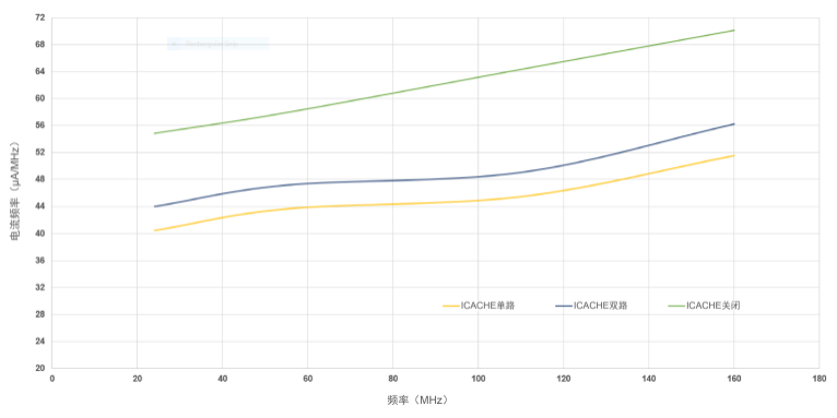
Figure 3. Power efficiency under various ICACHE configurations (SMPS, prefetch enabled, VDD=1.8V)
2.3 Flash Efficiency
The figure below shows the Flash latency (wait for state value to be programmed into the Flash access control register) depending on the STM32U575/585 regulator voltage regulation range and system clock frequency.
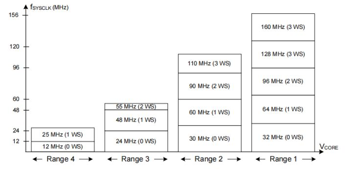
Figure 4. Flash latency vs. V core range (CVop=1.71-3.6V, LPM=0)
Flash supports Low Power Read Mode (LPM). The number of wait states (WS) depends on the LPM.
LPM=O up to 4 wS (depending on supply voltage and frame rate)
LPM=1 (reduced power consumption and increased latency): up to 15WS (depending on supply voltage and frequency)
This application note is for the STM32U575/585 microcontrollers based on the Arm® Cortex® core.
Ⅲ STM32U575/585 Ultra-low Power Consumption Characteristics
3.1 Low Power Mode
The STM32U575/585 microcontrollers implement several different power modes. By default, the MCU enters run mode after a system reset or power-on reset. The system provides several low-power modes to save power when the CPU does not need to be running, such as waiting for external events. The specific mode is selected by the user to find the best balance between low power consumption, short startup time, and available wake-up sources. For more detailed information, please refer to [1].
3.1.1 Sleep Mode
With the CPU clock off, all peripherals including the Cortex-M33 core (e.g. NVIC, SysTick, etc.) can run and wake up the CPU on interrupts or events.
3.1.2 Shutdown Mode
Stop mode is based on the combination of Cortex-M33 deep-sleep mode and peripheral clock gating. All clocks in the core domain are stopped. PLL, MSIS, MSIK, HSI16, and HSE oscillators are disabled and MSIS, MSIK, and HSI16 can be enabled in Stop 0, Stop 1, or Stop 2 modes if requested by the peripheral.
Shutdown 0 and Shutdown 1 provide the maximum number of active peripherals and wake-up sources, with shorter wake-up times and higher power consumption than Shutdown 2. In shutdown 2 and shutdown 3 modes, most of the core domain is in low-leakage mode.
On exit from Stop mode, the system clock can be MSIS (up to 24 MHz) or HSI16, depending on software configuration.
Low Power Background Autonomous Mode (LPBAM)
Some peripherals are autonomous and can run in Stop 0, Stop 1, or Stop 2 modes by requesting their core clock (MSIK up to 24MHz, or HSI16) and their bus (APB or AHB) when required, to communicate with DMA (GPDMA1 or LPDMA1, depending on peripheral and power mode) transfers data.
3.1.3 Standby Mode
Some peripherals are autonomous and can run in Stop 0, Stop 1, or Stop 2 modes by requesting their core clock (MSIK up to 24MHz, or HSI16) and their bus (APB or AHB) when required, to communicate with DMA (GPDMA1 or LPDMA1, depending on peripheral and power mode) transfers data.
3.1.4 Shutdown Mode
Power consumption is minimized in shutdown mode. This model is based on deep-sleep mode, where the voltage regulator is disabled. So the core domain is powered down. This mode achieves the lowest current consumption by shutting down the internal voltage regulator and disabling power consumption monitoring. Wake-up from this mode is possible via one of the five wake-up pins or the reset pin. The RTC clocked by the Low-Speed External Oscillator (LSE) is also functional in this mode with a wake-up function.
The "Summary of Low Power Modes" table in the "Power Modes" section of the document [1] summarizes the features available for each mode and provides an indication of the current consumption.
3.2 Power consumption optimization
3.2.1 ICACHE IN RUN MODE
ICACHE reduces power consumption by fetching instructions from internal ICACHE. In most cases, applications with lower performance profiles and strict low power constraints may benefit from the lower power consumption of ICACHE configured as direct-mapped (ICACHE_1-way).
This one-way cache configuration is achieved by programming WAYSEL=0 in ICACHE_CR.
3.2.2 Flash in run and sleep mode
The STM32U575/585 Flash includes a main memory block consisting of two 1 MB banks, each bank containing 128 8 KB pages. This structure is optimized for power consumption in dedicated mode when the MCU is in run and sleep mode. To reduce power consumption in the Run and Sleep modes, each bank can be put into power-down mode independently by setting PDREQ1 or PDREQ2 in FLASH_ACR, depending on the bank used.
Flash supports low-power read mode, by programming LPM=1 in FLASH_ACR to reduce power consumption.
Prefetching often improves code execution performance at the cost of additional Flash accesses. However, for most applications, power efficiency is better with prefetch turned on.
3.2.3 Power Control Optimization
In standby mode, the BOR can be configured in discontinuous mode (ultra-low power mode) to further reduce current consumption by setting the ULPMEN bit in PWR_CR to 1.
To reduce power consumption in Run, Sleep, or any low-power mode, it is recommended to switch from LDO to SMPS.
- SMPS supply pins are only available on certain packages with the SMPS buck converter option.
- SMPS to LDO and LDO to SMPS switching can be done dynamically.
3.2.4 RCC in Low Power Mode
To maintain the output clock accuracy, the MSI bias defaults to continuous mode. When the regulator is in Range 4 and the device is in Shutdown 1 or Shutdown 2 mode, setting MSIBIAS in RCC_ICSCR1 before entering low power mode reduces MSI power consumption.
Before entering the low-power mode, it is recommended to select HSI16 or MSIS (16 or 24MHz) as the wake-up source to shorten the wake-up time and reduce the energy lost during wake-up. If 24 MHz is used, a wait-state delay must be configured for SRAM read accesses, which affects code execution performance. The performance must then be evaluated between using 24 MHz with 1 SRAM wait state and using 16 MHz as the system clock.
The MSIS frequency during or upon wake-up from stop mode is the same as it was before entering stop mode. If the MSIS is used to feed the PLL in run mode, the MSIS is between 4MHz and 16MHz due to the PLL input clock frequency limitation. At this point, it is recommended to turn off the PLL and configure the MSIS to high frequency (if using MSIS as a wake-up clock) before entering shutdown mode.
All peripherals that cannot be enabled in Stop 2 must be disabled by clearing their own enable bits, or by configuring the RCC registers to be reset.
Each clock source, can be turned on or off individually when not in use to reduce power consumption.
3.2.5 I/O states in low-power modes
For more detailed information, please refer to [3].
Configure untapped GPIOs.
A GPIO always has an input channel, which can be digital or analog. If you do not need to read GPIO data, it is preferred to configure it as an analog input. This saves the consumption of input Schmitt triggers.
Disable GPIO register clock
If a GPIO group does not need to be used for a long time, please use the HAL_RCC_GPIOx_CLK_DISABLE() function to disable its clock.
Configuring GPIOs when entering low-power mode
In some applications, it is recommended to use an external pull-up instead of an internal pull-up to further reduce power consumption in shutdown mode and to obtain better resistor value accuracy.
3.2.6 Internal SRAM
The STM32U575/585 devices embed five SRAMs, each with a specific function: SRAM1, SRAM2, and SRAM3 are the main SRAMs. SRAM4 is used in SRAM for Peripheral Low Power Background Autonomous Mode (LPBAM) in Stop 2 mode.
All SRAM and register contents are retained, but SRAM can be fully or partially turned off to further reduce power consumption. These SRAMs consist of multiple blocks that can be turned off:
- Operating mode
To reduce power consumption in Run mode, all SRAM should be turned off by programming SRAMxPD in PWR_CR1.
- Shutdown mode
This mode achieves the lowest power consumption while maintaining the contents of the SRAM and registers powered by the low-power regulator. Shutdown 3 is the lowest power mode with full reservations. To further optimize power consumption, the following recommendations are recommended:
– Turn off unused SRAM by programming SRAMxPDSy = 1 in PWR_CR2:
◦ SRAM1, SRAM3, SRAM4
◦ DCACHE1、DMA2D、FDCAN、FMAC、PKA.
Depending on the application data size, reserve SRAM2 page 1 and/or page 2 by clearing the SRAMPDS1 and/or SRAMPDS2 bits in PWR_CR2.
- Standby Mode
After entering standby mode, except for the registers and backup SRAM (2 KB) in the backup domain and standby circuit, the contents of the rest of the SRAM and registers will be lost. SRAM2 page 1 (8 KB) or page 2 (56 KB) or both can be held in standby mode by setting RRSB1 and/or RRSB2 powered by low power regulators in PWR_CR1 (in RAM2 hold down standby).
3.2.7 Peripheral Clock Gating in Run and Stop Modes
STM32U575/585 devices support turning off the AHB/APB clock to further reduce power consumption.
When no AHB/APB peripheral is used and its clock is disabled, the following occurs:
- When setting AHB1DIS = 1 in RCC_CFGR2, all clocks to AHB1 peripherals are off (except BKPSRAM, DCACHE1, FLASH, ICACHE and SRAM1).
- When setting AHB2DIS = 1 in RCC_CFGR2, all clocks to AHB2 peripherals from RCC_AHB2ENR1 are turned off (except SRAM2 and SRAM3).
- When setting AHB3DIS = 1 in RCC_CFGR3, all clocks to AHB3 peripherals are turned off (except SRAM4).
- When setting APB1DIS = APB2DIS = 1 in RCC_CFGR2 and APB3DIS = 1 in RCC_CFGR3, all clocks to APB1/2/3 peripherals are turned off.
When a peripheral is enabled, its clock can be turned off automatically when the device is in Sleep mode by clearing the peripheral SMEN bits in RCC_AHBxSMENR and RCC_APBxSMENR. Both the EN bit and the SMEN bit of the peripheral must be set to 1 to keep the clock on in Sleep mode.
The peripheral's SMEN bit is also used to allow the peripheral to provide clocks in Stop 0 and Stop 1 mode upon request by the peripheral. When a peripheral requests a clock, that clock is distributed to all enabled peripherals. Therefore, if the peripheral is not used in Stop mode, the SMEN bit must be cleared before entering Stop mode.
Caution: The peripheral's SMEN bit must be set to enable the generation of a interrupt capable of waking the device from Stop mode.
3.3 Optimizing Peripheral Power Consumption Using LPBAM
The STM32U575/585 devices support Low-Power Background Autonomous Mode (LPBAM), which enables peripherals to operate and remain autonomous in Stop 0, Stop 1, and Stop 2 modes (without any software running).
This feature is available in Stop mode because of the performance of the peripheral request from its own independent clock, called the core clock. The core clock is automatically turned on when there is a peripheral request and automatically turned off when there is no peripheral request. For more detailed information, please refer to [1].
3.3.1 Peripherals supporting LPBAM
The table below lists all STM32U575/585 peripherals that support LPBAM.
Table 5: Peripherals supporting LPBAM
| Low Power Mode | Peripherals |
| Stop 0 or Stop 1 | ADC4、ADF1、DAC1、GPDMA1、LPDMA1、LPTIMx (x=1-4)、LPUART1、MDF1、I2Cx (x=1-4)、SPIx (x=1-3)、USARTx (x=1-5) |
| Stop 2 |
ADC4、ADF1、DAC1、LPDMA1、LPTIM1、LPTIM3、LPUART1、12C3、SPl3 |
3.3.2 Main Examples
The following are examples of use cases that can be done while left in shutdown mode (see document [4] for more details):
- ADC or DAC conversion triggered by a low-power timer (or any other trigger)
- Audio digital filter data transfer into SRAM: Wake-up from shutdown when sound activity is detected
- I2C/SPI slave transfer, UART/LPUART receive: wakeup at end of peripheral transfer or on DMA buffer event
- I2C/SPI master transfers triggered by LPTIM trigger (e.g. sensor periodic read), UART/LPUART transfers: wakeup at end of peripheral transfer or on DMA buffer event
- A bridge between peripherals. Example: ADC conversion data transmitted by communication peripherals
- Data transfer from SRAM to another SRAM
Ⅳ Selection Method of Low Power Consumption Mode
Consider a simplified application model where the application wakes up every Tperiod, always performs the same operation, and treats the number of instructions as constant (no wait loops, no data dependencies). The following approximate calculations can then be made:
- PROCESS phase duration (Tprocess) can be defined by the number of clock cycles (NOC) each phase is to execute. Defining FCLK as the CPU system clock frequency, the duration of the PROCESS phase is equal to TPROCESS = NOC / FCLK. The average current consumption in this phase is equal to the Tprocess.
- The duration of the INACTIVE phase is TPERIOD - PROCESS and its average current consumption are INACTIVE.
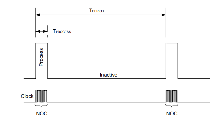
Figure5: Application Timing and Parameters
In order to obtain the average current consumption, the power consumption in the PROCESS phase and the INACTVE phase has to be summarized as follows:
The duration of the PROCESS phase is proportional to the number of clock cycles to execute (constant in the use case):
The model does not consider power consumption during the transition from the INACTIVE phase to the PROCESS phase, described in Section 4.5. Two parameters need to be chosen to optimize the average power consumption:
- The operating mode and clock frequency to be used in the PROCESS
- Low power mode to be used in the INACTIVE
4.1 PROCESS
Depending on the processing requirements (DMIPS), one of the following modes can be used:
- Run mode with Range 1 voltage up to 240 DMIPS at 160 MHz
- Run mode with Range 2 voltage up to 165 DMIPS at 110 MHz
- Run mode with Range 3 voltage, up to 82.5 DMIPS at 55 MHz
- Run mode with Range 4 voltage, up to 37.5 DMIPS at 25 MHz
Another parameter to consider when selecting a frequency is the ability to support the associated peripheral constraints.
4.2 INACTIVE
- sleep
- Shutdown 0 (main regulator on)
- Shutdown 1 (with low power regulator)
- Shutdown 2 (with low power regulator)
- Shutdown 3 (with low power regulator)
- Standby (with RTC and SRAM2 retention options)
- Shutdown (with RTC as an option)
Depending on the wakeup source and sleep cycle duration, one of the following modes can be selected:
- Sleep: if reactivity is a critical parameter (wakeup time is only 8 system clock cycles at this point)
- Shutdown 0: When wake-up time is critical (<2.5μs if the program resides in Flash)
- Shutdown 1: If multiple peripherals need to keep awake and the system has multiple wakeup sources (the application must be able to tolerate about 13 & mu's wakeup time from Flash)
- Halt 2: If few peripherals need to stay awake and can generate wake-up events, such as DMA transfer complete, LPUART/SPI/I2C µs wake-up time from Flash)
- Shutdown 3: 66.5 & micro's wakeup from Flash with FSTEN = 0 if no peripherals other than RTC need to stay awake with all SRAM preserved
- Standby: If no other peripherals need to keep awake except RTC, and no more than 64 KB of SRAM2 needs to be reserved (the application must allow about 64.5 & mu's wake-up from Flash when MSIS = 4 MHz and FSTEN = 0 )
- Shutdown: if only the RTC and backup registers need to stay awake (then the application must tolerate ~610 μs wakeup time at MSIS = 4 MHz)
Wake-up time depends on code location (Flash), system clock source, and frequency. Please refer to [2] for details. The graph above for wake from shutdown corresponds to MSIS at 24MHz or 4 MHz and the code is in Flash. To shorten the wake-up time, it is recommended to set FLASHFWU = 1 and SRAM4FWU = 1 in PWR_CR2.
4.3 Sleep mode selection
The following numerical results are based on typical specification values at 25°C extracted from the document [2].
For the different selected low-power modes (sleep, shutdown 1, shutdown 2, shutdown 3, standby with RTC and SRAM2 retention function, standby and shutdown) when the RTC is in the INACTIVE stage, the following figure shows the main power supply (VDD ) Theoretical power consumption of the function.
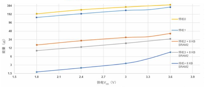
Figure6: Impact of Low Power Mode on Average Energy Consumption (LDO)
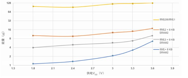
Figure7: Impact of Low Power Mode on Average Power Consumption (SMPS)
The preceding graphs show that for applications that need to retain some data, standby mode provides the best power consumption, while shutdown 3 mode is the lowest power mode that preserves all SRAM. As shown in Figure 7, using an SMPS cuts energy consumption in half.
Shutdown mode (dotted line) was discarded because it does not provide sufficient data retention for this type of application.
Low power mode selection is determined not only by overall power consumption but also by other wake-up considerations connected to the application. Figure 6 and Figure 7 show that compared to Standby, Stop 2 and Stop 3 modes are more robust, simple, and fast to set up for wake-up (no need for peripheral re-initialization) at the cost of a small amount of additional power consumption.
4.4 Low Power Mode Selection
For practical applications, depending on the wake-up period, the following guidelines can be used:
- If the wake-up period is longer than tens of ms, use standby mode to achieve better power consumption performance.
- If the wake-up period is short, a shutdown 2 or shutdown 3 mode implementation is better.
- Standby mode is best used if the temperature is high.
Low-power mode selection depends on power consumption and wake-up time requirements (system reactivity) and data retention requirements. If the processing can be accommodated below 24 MHz, the advantages are as follows:
- Standby or shutdown 3 modes
In standby mode, the sweet spot is a wake-up transition time longer than 66μs and a reserved area lower than 64KB SRAM + 2KB BKPSRAM. In Stop 3 mode, all SRAM can be reserved.
- Shutdown 2 mode
The sweet spot is that the wake-up transition time is longer than 20μs and the reserved area is larger than 66KB (64KB SRAM2 + 2KB BKPSRAM) reserved.
Shutdown mode has the best power performance if the wake-up period is longer than a few seconds and no memory needs to be preserved. The typical wake-up time, in this case, is 610µs.
4.5 Impact of conversion
To complete this study, the energy expended during the transition phase (wake up and deactivate) had to be considered.
According to the document [2], when VDD=3.0V, using SMPS, the energy consumed when leaving the low-power mode is rough:
- 1.1 nAs for the transition from Stop 1 to Run mode (MSI = 24 MHz)
- 0.57 nAs for transition from Stop2 to Run mode (MSI = 24 MHz)
- 4.54 nAs for transition from Stop3 to Run mode (MSI = 24 MHz)
- 21.22 nAs for a transition from standby to run mode (MSI = 4 MHz)
- 457.29 nAs for a transition from shutdown to run mode (MSI = 4 MHz)
Ⅴ Conclusion
This article describes the ultra-low power features of the STM32U575/585 microcontrollers. They show the benefits of this microcontroller family in reducing current consumption in embedded systems. Regardless of the application, these devices offer options for optimizing performance and power consumption.
 Tesla cuts 10% of global layoffs, Samsung increases NAND flash memory production this quarter4/17/2024 22
1.Tesla announced 10% of its global layoffs, with a higher domestic proportion
Read More > How much do you know about fpga design engineer?4/16/2024 34
Circuitry can be a complex field. The circuit must be completely redone because even the smallest error can drastically alter the project's outcome. One of the numerous individuals involved in circuit building is the FPGA design engineer.An electrical engineer with a focus on designing Field Programmable Gate Array integrated circuits is known as an FPGA engineer.After reading this site, you will be fully informed about fpga design engineers.
Read More > Renesas starts up old factory to increase power device production4/15/2024 19
Renesas Electronics announced in December that the Kofu factory that had previously ceased operations was reactivated. As a 300mm wafer fab, the plant will begin mass production of IGBTs and other products in 2025, doubling Renesas' current power semiconductor production capacity. Renesas held an opening ceremony on April 11, which was attended by local government officials and partner companies.
Read More > 5 key points of Xilinx Artix7 hardware design4/12/2024 32
The following mainly discusses four aspects of the Artix7 chip based on experiences: main chip power supply circuit, selection of main chip filtering capacitors, bank voltage and pin configuration, peripheral circuit construction, and PCB hardware design. These are all summaries obtained after practice, hoping to inspire and help others in their work and study.
Read More > Microchip enabling capacity at TSMC's Kumamoto factory, causing a price increase for Micron products4/11/2024 36
Microchip expands cooperation with TSMC and will establish a 40-nanometer production line at the Kumamoto factory
Read More >
Hot News
- Diode Overview: Application in Automotive Alternator Rectifiers
- Ultra-low power consumption of STM32U575/585 microcontrollers(MCU)
- The Best Guide to Transistor
- Basic Information about Temperature Sensor
- Electronic Component Symbols: Resistor, Capacitor, Transformers and Connectors
- Voltage-Controlled Oscillator: Principle, Type Selection, and Application
SUPPORT
ABOUT BITFOIC
QUICK LINKS
Connect with us
Tel: 86-755-23606554
E-mail: contact@bitfoic.com
Address: Room A29, 24 / F, Hoi Tak Wai, Prince Edward industrial building, 706 Prince Edward Road East, San Po Kong, Kowloon,Hongkong
Mon-Fri: 09.30 AM - 18.30 PM


