


The Best Guide to Transistor
Introduction
The transistor is electronic equipment. It is made through a p and n-type semiconductor. When a semiconductor is placed in the center between the same type of semiconductors the arrangement is called a transistor. We can say that a transistor is the combination of two diodes it is a connection back to back. A transistor is a device that regulates current or voltage flow and acts as a button or gate for electronic signals.
NPN and PNP transistors explained. How does a transistor work? What is the difference between an NPN and a PNP transistor? We find out in this video.
Catalog
Ⅰ What is a Transistor?
Ⅱ How does a Transistor work?
Ⅲ What is the circuit of the Transistor?
ⅣDifferent Types of Transistors
4.1 BJT vs FET
4.2 BJT Transistor
4.2.1 NPN Transistor
4.2.2 PNP Transistor
4.2.3 NPN Transistor vs PNP Transistor
4.3 FET Transistor
4.4 JFET Transistor
4.5 MOSFET Transistor
ⅤApplications of Transistors
ⅥFrequently Asked Question
Ⅰ What is a Transistor?
Transistors, also known as Bipolar Junction Transistors (BJTs), are semiconductor devices driven by current to control the flow of current, where a small current in the base lead controls a large current between the collector and emitter. They can be used to amplify weak signals, such as oscillators or switches. Transistors are usually made of silicon crystals, with N and P-type semiconductor layers sandwiched together.
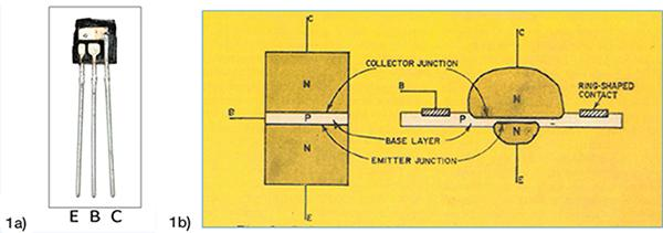
Figure1: cutaway view of a 2N3904 TO-92 and N and P-type lamellae
Figure 1: Figure 1a shows a cutaway view of a 2N3904 TO-92 showing the E - e-emitter, B - base, and C - collector leads connected to the silicon base. Figure 1b, taken from the May 1958 issue of Radio-Electronics, shows N and P-type lamellae and their arrangement (germanium was used at the time).
The transistor is hermetically sealed and packaged in a plastic or metal cylindrical case with three leads (Figure 2)
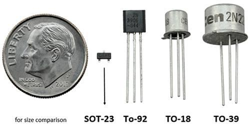
Figure 2: Comparison of various popular package types and sizes.
Ⅱ How does a Transistor work?
Take the NPN transistor as an example to illustrate the working principle of the transistor. To understand how these types of components work as switches, it's easy to imagine water flowing through a pipe controlled by a valve. The water pressure represents "voltage" and the flow of water through the pipe represents "current" (Figure 3). The large water pipe represents the collector/emitter junction, separated by a valve in the middle. The valve is represented by a gray oval in the figure, like a movable baffle, actuated by the water flow in the small water pipe representing the base. The valve maintains water pressure from the collector to the emitter. When the water flows through the smaller water tube (the base), it opens the valve between the collector/emitter junctions, allowing the water to flow through the emitter to the ground (the ground represents the return path for all water or voltage/current).
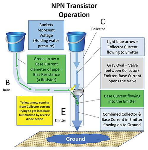
Figure 3: This figure illustrates graphically how a transistor works.
When water flows through the small water tube (base), it opens between the collector/emitter junction
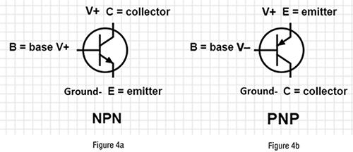
Figure 4: Schematic symbols for each transistor type.
After determining the bias voltage, the next variables required are the amount of voltage and current required for the load to operate. These variables will become the transistor's minimum voltage and current ratings. Tables 1 and 2 below provide some common transistors and their main specifications, including their voltage and current limits.
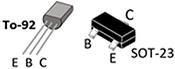
Figure5: Transistors, NPN and PNP, led and surface mount
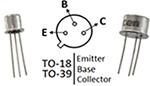
Figure6: Transistors, NPN and PNP, Metal Cylindrical Package
Ⅲ What is the circuit of the Transistor?
Figure 5 shows an example of a circuit where the collector-emitter junction is turned on by energizing the base, or by applying 5 volts to the base through a slide switch to bias the transistor to turn it on. This example will light an LED used as a load. When biasing the base, proper use of resistors is required to prevent overcurrent. Test the example circuit with the leaded parts in the breadboard. When most engineers use transistors in a new product design coming to market, they use surface mount components (much smaller than the TO-92 package size).
Since the 2N3904 is an NPN transistor, the base needs to be positively biased (proper voltage level and resistance) to open the collector-emitter junction for proper current flow. Also, the use of a load resistor (R1) is important so that too much current does not flow through the LEDs and transistors. See the 2N3904 data sheet for more information on this transistor.
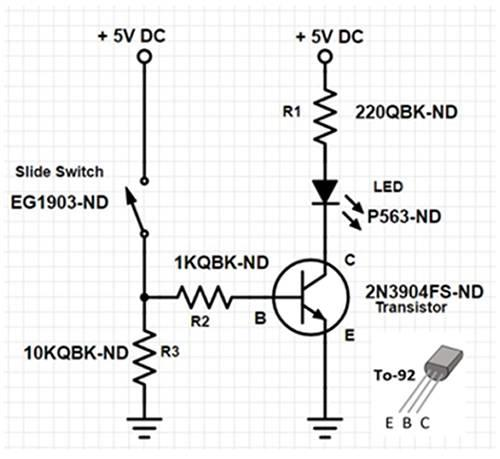
Figure 5: Example of a 2N3904 circuit using an EG1218 slide switch to light an LED, including C (collector), E
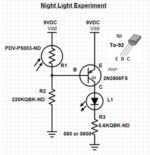
Figure 6: Example of a 2N3906 night light circuit using a PDV-P5003 photocell to light an LED
Ⅳ Different Types of Transistors
A transistor is made of a semiconductor and there are various types of transistors depending on their characteristics and has their advantages and disadvantages:
Some types of transistors are listed below:
Bipolar Junction Transistor
Diffusion Transistor
Avalanche Transistor
Schottky Transistor
Darlington Transistor
Heterojunction Bipolar Transistor
Field Effect Transistor
Junction FET Transistor
Dual Gate MOSFET
Multiple-Emitter Transistor
But, the main classification of transistors is as follows:
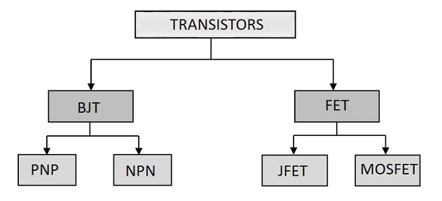
Figure7: common types of transistor
In the next few sections, let us study these transistors in detail.
4.1 BJT vs FET
There are two common types of Transistors. Bipolar Junction Transistors (BJT), are divided into NPN and PNP transistors, and Field Effect Transistors (FETs), are divided into JFETs and MOSFETs. Junction FET transistors are further classified into N-channel JFETs and P-channel JFETs based on their structure. MOSFETs are divided into depletion mode and enhancement mode. Likewise, depletion and enhancement mode transistors are further divided into respective N-channel and P-channel.
On a broader scale, as mentioned earlier, the main families of transistors are BJTs and FETs. Regardless of which series they belong to, all transistors have an appropriate/specific arrangement of different semiconductor materials. The semiconductor materials commonly used to make transistors are silicon, germanium, and gallium arsenide.
Transistors are classified according to their structure. Each type of transistor has its characteristics, advantages, and disadvantages. Physically and structurally, the difference between a BJT and a FET is that in a BJT, both majority and minority charge carriers are required to work, whereas, in the case of a FET, only the majority charge carriers are required. Based on their characteristics and characteristics, some transistors are mainly used for switching purposes (MOSFETs), and on the other hand, some transistors are used for amplifying purposes (BJTs). Some transistors are designed for amplification and switching purposes.
Figure8: types of transistor
4.2 BJT Transistor
Junction transistors are often referred to as bipolar junction transistors (BJTs). The term "bipolar" means that both electrons and holes are needed to conduct electric current, and the term "junction" means that it consists of a PN junction (actually two junctions).
A BJT has three terminals called emitter (E), base (B), and collector (C). BJT transistors are divided into NPN and PNP transistors according to their structure.
BJTs are essentially current-controlled devices. If a small number of current flows through the base of a BJT transistor, it causes a large current to flow from the emitter to the collector. Bipolar junction transistors have low input impedance, which causes high currents to flow through the transistor.
There are three operating regions of a bipolar junction transistor:
- Active region: The region in which the transistors operate as an amplifier.
- Saturation region: The region in which the transistor is fully on and operates as a switch such that the collector current is equal to the saturation current.
- Cut-off region: The region in which the transistor is fully off and the collector current is equal to zero.
4.2.1 NPN Transistor
NPNs are one of two types of bipolar junction transistors (BJTs). NPN transistors consist of two n-type semiconductor materials separated by a thin layer of p-type semiconductor. Here, the majority charge carriers are electrons while holes are the minority charge carriers. The flow of electrons from the emitter to the collector is controlled by the current in the base terminal.
A small amount of current at the base terminal causes a large amount of current to flow from the emitter to the collector. The more commonly used bipolar transistors are NPN transistors because the mobility of electrons is greater than that of holes. The standard equation for the current flowing through a transistor is
IE = IB + IC
The symbol and structure of an NPN transistor are shown below.
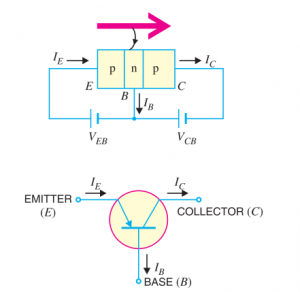
Figure9:symbol and structure of an NPN transistor
4.2.2 PNP Transistor
PNPs are another type of bipolar junction transistor (BJT). A PNP transistor consists of two p-type semiconductor materials separated by a thin layer of n-type semiconductor. The majority of charge carriers in a PNP transistor are holes, while electrons are the minority charge carriers. Arrows in the emitter terminals of transistors indicate the flow of conventional current. In a PNP transistor, current flows from the emitter to the collector.
A PNP transistor turns on when the base terminal is pulled low with respect to the emitter. The symbol and structure of a PNP transistor are shown below.
Figure9:symbol and structure of a PNP transistor
4.2.3 NPN Transistor vs PNP Transistor
Even though both NPN and PNP transistors are bipolar junction transistors, there are several differences between them. Transistors can be used as an amplifier and device switches in some situations. In a PNP transistor, the majority charge carriers are holes while in NPN, the majority charge carriers are electrons.
Unlike NPN, which switches ON by a high signal, PNP does so by a low signal. P stands for the polarity of the emitter terminal in PNP transistors, and N stands for the polarity of the base terminal.
In NPN, N stands for the material's negatively charged coating while P stands for the positively charged layer.
| NPN | PNP |
| The current flows from the collector terminal to the emitter terminal. | The current flows from the emitter to the collector terminal. |
| The two N-type semiconductors are surrounded by one P-type semiconductor. | It is constructed of two P-type material layers with an N-type layer in the middle. |
| By maintaining a +ve voltage in the collector, the current is produced there. | By maintaining a +ve voltage at the emitter terminal, the current is created from the emitter to the collector. |
| When the current in the base terminal increases, the transistor turns on. | When there is no current flowing at the base terminal, the transistors turn ON. |
| The transistor flips OFF and doesn't operate across the collector terminal when the base current is lowered. | A PNP transistor turns OFF when its base has a current flowing through it. |
4.3 FET Transistor
Field Effect Transistors (FETs) are another major type of transistor. Basically, a FET also has three terminals (like a BJT). The three terminals are Gate (G), Drain (D), and Source (S). Field effect transistors are divided into junction field effect transistors (JFETs) and insulated gate field effect transistors (IG-FETs) or metal oxide semiconductor field effect transistors (MOSFETs).
For connections in the circuit, we also consider a fourth terminal called the Base or Substrate. A FET can control the size and shape of the channel between the source and drain, which is created by the voltage applied to the gate.
Field Effect Transistors are unipolar devices because they require only a majority of charge carriers to operate (unlike bipolar transistors, BJTs).
4.4 JFET Transistor
The junction field effect transistor (JFET) is one of the earliest and simplest field effect transistors. JFETs are used as switches, amplifiers, and resistors. The transistor is a voltage-controlled device. It does not require any bias current.
A voltage applied between the gate and source controls the flow of current between the source and drain of the transistor. JFET transistors are available in N-channel and P-channel types.
N-channel JFET
In an N-channel JFET, the current flow is caused by electrons. When a voltage is applied between the gate and the source, a channel is formed between the source and the drain for the current to flow. This channel is called the N-channel. Today, N-channel JFETs are the preferred type over P-channel JFETs.
P-channel JFET
In this type of JFET, the current is induced by holes. The channel between the source and the drain is called P-channel.
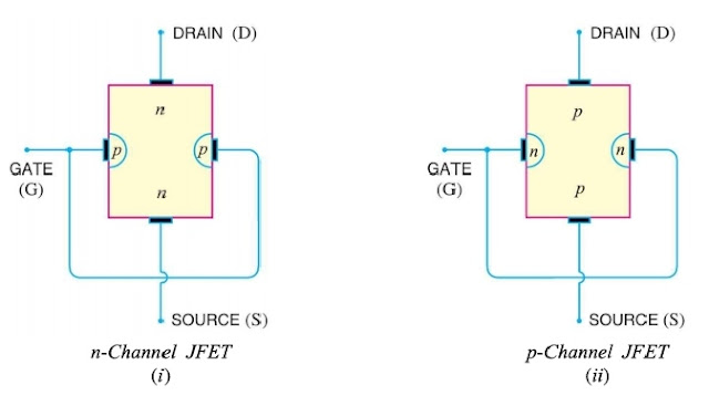
Figure10:symbol and structure of a JFET Transistor
4.5 MOSFET Transistor
Metal Oxide Semiconductor Field Effect Transistors (MOSFETs) are the most commonly used and popular type of all transistors. The name "Metal Oxide" means that the gate region and channel are separated by a thin layer of metal oxide, usually SiO2.
Hence, MOSFETs are also called insulated gate FETs because the gate region is completely insulated from the source-drain region. There is an extra terminal called the substrate or body, which is the main semiconductor (silicon) from which the FET is made. Hence, a MOSFET has four terminals drain, source, gate, and body or substrate.
MOSFET has many advantages over BJT and JFET, mainly it provides high input impedance and low output impedance. It is used in switching and power circuits and is a major component of integrated circuit design technology.
MOSFET transistors are available in depletion and enhancement modes. In addition, the depletion type and enhancement type are divided into N-Channel and P-Channel types.
N-channel MOSFET
A MOSFET with an N-channel region between the source and drain is called an N-channel MOSFET. Here, the source and gate terminals are heavily doped with n-type material in a heavily doped p-type semiconductor material (substrate).
The current flow between the source and drain is due to electrons. The gate voltage controls the current in the circuit. N-channel MOSFETs are more commonly used than P-channel MOSFETs because the mobility of electrons is higher than that of holes.
P-channel MOSFET
A MOSFET with a P-channel region between the source and drain is called a P-channel MOSFET. Here, the source and drain terminals are heavily doped with a P-type material, while the substrate is doped with an N-type material. The current flow between the source and drain is due to hole concentration. The voltage applied at the gate will control the current flowing through the channel region.
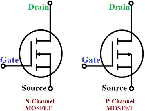
Figure10:symbol and structure of a MOSFET Transistor
ⅤApplications of Transistors
Understanding the maximum ratings and electrical characteristics of power semiconductors is necessary for proper application; these details are provided in the device datasheet. Datasheet limits are used in good design practice instead of information from small sample lots. A rating is a maximum or minimum figure that places a cap on the capability of the apparatus. Acts that go beyond a rating may cause irreparable deterioration or device failure. Maximum ratings denote a device's most advanced capabilities. They should not be used as design parameters.
A characteristic is a way to describe how well a device performs under specific operating conditions. It can be done graphically or by using minimum, characteristic, and/or maximum numbers.
Ⅵ Frequently Asked Questions
1. What are the 3 functions of transistors?
transistor, a semiconductor device for amplifying, controlling, and generating electrical signals.
2. Is a transistor AC or DC?
And here is a point that many people confuse: Transistors are NOT AC components: Transistors can only operate with DC signals!
3. Why transistor is used as a switch?
A transistor can be extensively used for switching operations either for opening or closing a circuit. Meanwhile, the basic concept behind the operation of a transistor as a switch relies on its mode of operation. Generally, the low-voltage DC is turned on or off by transistors in this mode.
4. Can transistors generate electricity?
Transistors do not create electric current, they only control the electric current supplied to them. The input current at the base controls the output current flowing between the emitter and the collector. The transistor can turn on or off if the base current turns on or off.
5. Why capacitor is used in transistors?
They are used to prevent interference of a transistor's bias voltage by AC signals. In most amplifier circuits, this is achieved by driving the signal to the base terminal of a transistor through a coupling capacitor.

 A Comprehensive Guide to Grasping FPGA Structure6/20/2024 894
FPGA (Field-Programmable Gate Array) is an integrated circuit, a type of programmable chip, that allows engineers to program custom digital logic. It can change its hardware logic based on the program, with the primary purpose of enabling engineers to redesign and reconfigure their chips faster and cheaper, whenever they want. However, nothing in the world is ideal, and FPGA chips also have limitations!
Read More > The EU to Impose Tariffs on Electric Vehicle Imports from China in Early July6/17/2024 423
The EU to Impose Tariffs on Electric Vehicle Imports from China in Early July
Read More > What is XC7A100T-2FG484I?6/6/2024 637
XC7A100T-1CSG324C is an FPGA-based digital signal processing board, which consists of Xilinx's Virtex-7 series chips and FPGA interface chips.
Read More > Analog cycle inventory hits bottom, AI drives flash memory demand to continue6/4/2024 666
Analog cycle inventory hits bottom, AI drives flash memory demand to continue
Read More >
Hot News
- Electronic Component Symbols: Resistor, Capacitor, Transformers and Connectors
- Diode Overview: Application in Automotive Alternator Rectifiers
- Ultra-low power consumption of STM32U575/585 microcontrollers(MCU)
- Voltage-Controlled Oscillator: Principle, Type Selection, and Application
- What is Xilinx 7 Series FPGA Clock Structure- -Part two
- Zedboard zynq-7000: Zynq 7000 datasheet, Features, Architecture and Core Components
SUPPORT
ABOUT BITFOIC
QUICK LINKS
Connect with us
Tel: 86-755-23606554
E-mail: [email protected]
Address: Room A29, 24 / F, Hoi Tak Wai, Prince Edward industrial building, 706 Prince Edward Road East, San Po Kong, Kowloon,Hongkong
Mon-Fri: 09.30 AM - 18.30 PM


