


Voltage-Controlled Oscillator: Principle, Type Selection, and Application
Introduction
Many electronic applications require changing the frequency of one signal based on the magnitude of another signal. A good example is a frequency-modulated signal, where the carrier frequency varies with the amplitude of the modulating source. Also, there is a phase-locked loop (PLL): a circuit that uses a control system to change the frequency and/or phase of an oscillator to match the frequency/phase of an input reference signal.
Catalog
ⅠWhat is the Function of VCO?
ⅡHow does a VCO Work?
Ⅲ Types of Voltage-Controlled Oscillators
Ⅳ Voltage Controlled Oscillator – Practical Application
Ⅴ Specify VCO
Ⅵ Modular VCO
Ⅶ Monolithic VCO
Ⅷ FAQ about Voltage-Controlled Oscillator
ⅠWhat is the Function of VCO?
Many electronic applications require changing or controlling the frequency or phase of one signal based on the magnitude of another signal. Typical applications include communication systems, frequency chirping in radar, phase tracking in PLLs, and frequency-hopping applications such as remote keyless entry (Figure 1).

Figure 1: Examples of applications that require the control of frequency or phase changes by applying a voltage signal include: frequency modulation in communication systems (above), frequency chirping in radar (second image below), phase in phase-locked loops Tracking (third image below) and frequency hopping applications such as remote keyless entry systems (below). (Image source: Digi-Key Electronics)
A VCO is designed specifically to produce an output signal whose frequency varies within a reasonable range based on the amplitude of the input signal.
Ⅱ How does a VCO Work?
VCOs come in discrete, modular, and monolithic forms, but a discussion of discrete VCOs will help readers get a basic understanding of how they work and why certain metrics are important. Afterward, we briefly describe modular and monolithic solutions. Using a discrete VCO gives designers extreme flexibility to meet custom specifications. This method is especially common in do-it-yourself (DIY) projects, especially in the field of amateur radio. These designs are used in high-frequency radio projects and are based on classic oscillator topologies, including the Hartley and Colpitts inductor-capacitor (LC) oscillator (Figure 2).
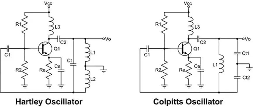
Figure 2: Classic oscillators include Hartley and Colpitts LC oscillators, which can serve as the basis for VCO designs. (Image
source: Digi-Key Electronics)
All oscillators are based on the use of positive feedback to achieve continuous oscillation. The Hartley and Colpitts oscillators are the basic designs, which generate positive feedback in different ways. Positive feedback requires that the signal from the oscillator output be returned to the input with a total phase shift of 360° The amplifier provides 180° phase inversion, and the other half of 360° comes from the LC of the oscillator circuit. The oscillator circuit determines the nominal oscillation frequency. In the Hartley oscillator circuit, the oscillator circuit consists of L1, L2, and Ct; in the Colpitts oscillator, the oscillator circuit consists of L1, Ct1, and Ct2.
Hartley oscillators are inductively coupled, and phase inverting is achieved through a double or tapped inductor (L1 and L2) as shown in the circuit. The Colpitts oscillator uses a capacitive voltage divider consisting of Ct1 and Ct2 in the corresponding circuit. Many designs were derived from these basic designs, each with its own name. These derivative designs attempt to isolate the oscillator circuit from the amplifier to prevent frequency shifts due to loading. There are many such derivative designs, and designers can choose their favorite ones.
Frequency control is added to these designs by using varactor diodes, which are junction diodes designed to provide variable capacitance, to change the resonant frequency of the tank circuit. The P-N junction is reverse-biased and the capacitance of the diode can be changed by changing the applied DC bias voltage. The capacitance of a varactor diode is inversely proportional to the applied DC bias voltage: the higher the reverse bias, the larger the depletion region of the diode and thus the lower the capacitance. This change can be seen in the capacitance reverse voltage plot of the SMV1232_079LF hyper abrupt junction varactor from Skyworks Solutions (Figure 3). This diode has a capacitance of 4.15 picofarads (pF) at zero voltage and 0.96pF at 8V.
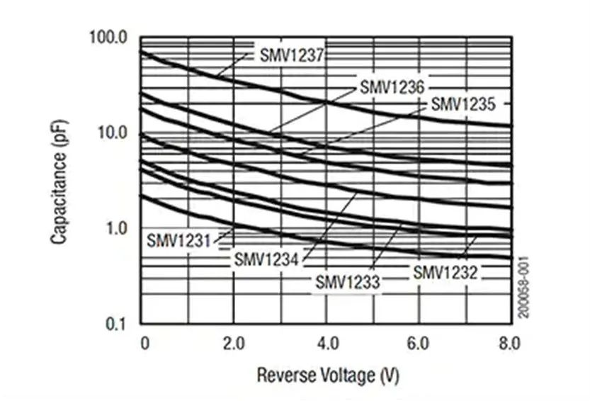
Figure 3: The voltage-capacitance plot of Skyworks Solution's SMV1232 varactor diode clearly shows how the capacitance changes inversely with the applied DC bias voltage. (Image source: Skyworks Solutions)
The capacitance range of the varactor determines the tuning range of the VCO. The voltage control of the oscillator is achieved by adding a rheostat in parallel with the oscillation circuit, as shown in Figure 4. Shown is an evaluation board reference design for a Colpitts oscillator VCO with a center frequency of 1 gigahertz (GHz) and a tuning range of approximately 100 megahertz (MHz). This reference design integrates an emitter follower buffer to isolate the VCO from load changes. The resonant circuit in this design includes inductance L3 and electric capacities C4, C7, and C8. Varactor diode VC1 is connected in parallel with the oscillation circuit. Capacitor C4 controls the frequency range for a given varactor, while C7 and C8 provide the feedback needed to maintain oscillation.
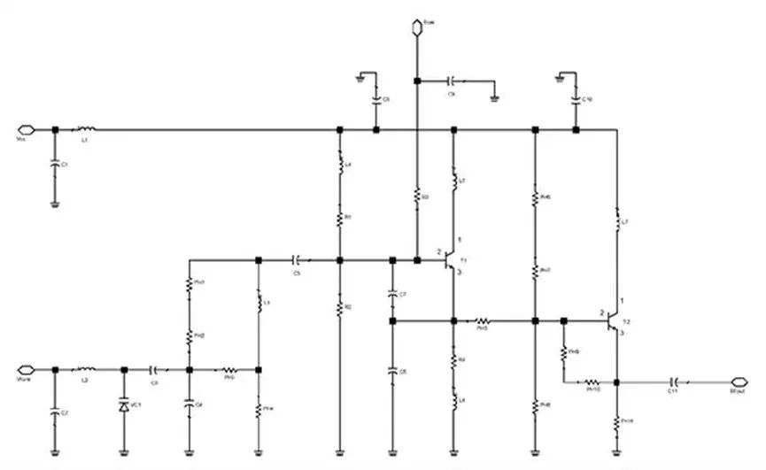
Figure 4: An evaluation board reference design for a Colpitts oscillator VCO with a center frequency of 1GHz and a tuning range of about 100MHz. The varactor diode VC1 (lower left) is connected in parallel with the oscillator circuit and consists of an inductor L3 and capacitors C4, C7, and C8. (Image source: NXP Semiconductors)
The choice of varactors and bipolar junction transistors depends on the oscillator frequency. For a nominal frequency of 1GHz, an RF transistor such as the BFU520WX from NXP Semiconductors or the BFP420FH6327XTSA1 from Infineon Technologies can be used. The BFU520WX has a transition frequency of 10GHz and a gain of 18.8 decibels (dB), and the BFP420FH6327XTSA1 has a transition frequency of 25GHz and a gain of 19.5dB. Both have enough gain-bandwidth product at 1GHz to accommodate this circuit.
In summary, discrete VCOs offer the greatest design flexibility, but are larger and require more PCB area than modular or monolithic devices.
Ⅲ Types of Voltage-Controlled Oscillators
There are many types of VCO circuits used in different applications, but they can be broadly classified into two types based on their output voltage.
Harmonic Oscillators: If the Output waveform of the oscillator is sinusoidal then it is called a harmonic oscillator. The RC, LC circuits, and Tank circuits fall into this category. These types of oscillators are harder to implement but they have better stability than the Relaxation Oscillator. Harmonic oscillators are also called linear voltage-controlled oscillators.
Relaxation Oscillator: If the output waveform of the oscillator is in the sawtooth or triangular form then the oscillator is called a Relaxation Oscillator. These are comparatively easy to implement and hence most widely used. Relaxation Oscillator can further be classified as
- Emitter Coupled Voltage Controlled Oscillator
- Grounded capacitor Voltage Controlled Oscillator
- Delay-based ring Voltage Controlled Oscillator
Ⅳ Voltage Controlled Oscillator – Practical Application
As was already indicated, a VCO can be easily built using an RC or LC pair, but in practical applications, nobody really does that. A specific type of integrated circuit (IC) can produce oscillations based on the input voltage. The LM566 from National Semiconductor is one such widely utilized integrated circuit.
This IC can produce square and triangular waves, and a resistor and external capacitor can be used to adjust the wave's nominal frequency. Later, dependent on the input voltage supplied to it, this frequency can also be changed in real-time.
The pin diagram of the LM566 IC is shown below
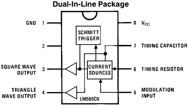
A single supply or two supply rails with an operating voltage of up to 24V can be used to power the IC. The output pins, 3, and 4, respectively, provide us with a square wave and a triangle wave. By connecting the appropriate value of a capacitor and resistor to pins 7 and 6, the nominal frequency can be adjusted.
The formulae to calculate the value of R and C based on the output frequency (Fo) are given by the formulae
Fo = 2.4 (Vss - Vc) / Ro+Co+Vss
Where,
Vss is the supply voltage (here 12V) and Vc is the control voltage applied to pin 5 based on whose magnitude the output frequency is controlled. (Here we have formed a potential divider using 1.5k and 10k Resistor to supply a constant voltage to pin 5). A sample circuit diagram for LM566 is shown below.
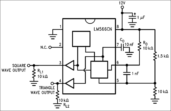
In real-world applications, the 1.5k and 10k resistors can be disregarded, and pin 5 can receive the control voltage directly. In accordance with the desired output frequency range, you can also alter the values of Ro and Co. To determine how linearly the output frequency varies in relation to the input control voltage, consult the datasheet as well. We can provide a wide range of control by using the Control voltage (on pin 5) to modify the output frequency value in a 10:1 ratio.
Ⅴ Specify VCO
The main VCO specifications usually start from the nominal frequency range, which is the lowest and highest frequency that can be obtained. Alternatively, these parameters can also be specified as nominal or center frequency and tuning range.
The input tuning voltage range corresponds to the input voltage swing over which the VCO is tuned (Figure 5).
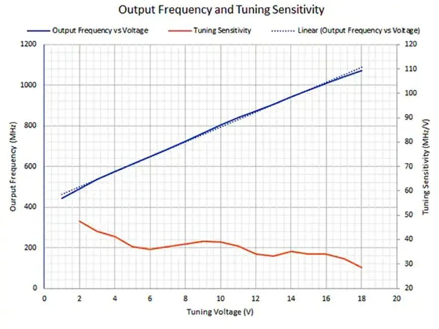
Figure 5: The tuning plot of output frequency as a function of input tuning voltage gives you a basic idea of VCO linearity compared to a linear fit. The slope of the output frequency and tuning voltage is the tuning sensitivity. (Image source: Digi-Key Electronics)
Tuning gain or sensitivity is simply the slope of the frequency-voltage curve in MHz/volt (V). This is a measure of tuning linearity. In applications where the VCO is in the control loop, such as a PLL, the tuning sensitivity is the gain of the VCO components and can affect the dynamic performance and stability of the control loop.
The output power of a VCO specifies the power delivered to a load of a specified impedance, typically 50 ohms (Ω) for RF VCOs. Output power is given in dB, referenced to 1 milliwatt (mW) (dBm). The flatness of the power output is also of concern over the frequency range of the VCO.
Load pull is the change in VCO output frequency due to a change in load impedance and is measured in MHz peak-to-peak (pk-pk). Typically, load isolation is improved by using a buffer amplifier like the emitter follower shown in Figure 4.
Power boosting is a phenomenon in which the VCO output frequency changes due to changes in the power supply voltage. Its unit is MHz/V.
The phase noise specification is an indicator of the purity of the VCO signal. The spectrum of an ideal oscillator is a narrow spectrum of lines at the oscillator frequency. Phase noise represents unwanted modulation of the oscillator and broadens the spectral response. Phase noise is the result of heat and other noise sources within the oscillator circuit and is expressed in decibels per hertz below the carrier (dBc/Hz). Phase noise in the frequency domain can cause timing jitter in the time domain, manifested as time interval error (TIE).
Ⅵ Modular VCO
Modular VCO represents the next highest level of circuit integration. These VCOs are housed in small, modular housings that can be used as components. Modular VCOs typically have a higher packing density than discrete VCOs. These devices are available in a range of output frequencies, tuning ranges, and power output levels. An example is the CRBV55BE-0325-0775VCO from Crystek Corporation (Figure 6). The device measures 1.25 x 0.59 inches (in.) (31.75 x 14.99 millimeters (mm)) by 1.25in. height has an input voltage range of 0 - 12 volts, and a tuning range of 325 - 775MHz. Its output power level is +7dBm (typical) and its phase noise is -98dBc/Hz at 10 kilohertz (kHz) carrier offset and -118dBc/Hz at 100kHz.
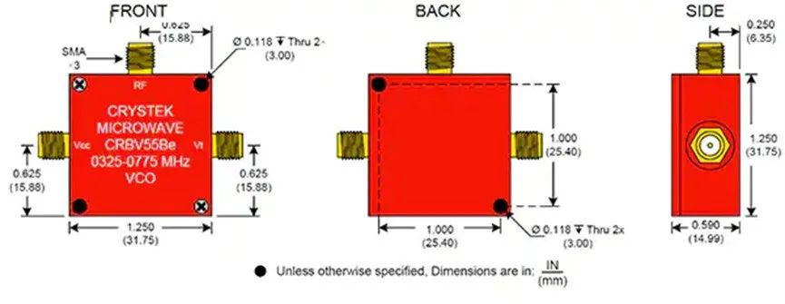
Figure 6: Outline drawing of the Crystek CRBV55BE VCO showing its compact form factor of 1.25 x 1.25 x 0.59in. (Image source: Crystek Corporation)
In terms of dynamic control, the typical tuning sensitivity of the Crystek VCO is 45MHz/V. Power boost is specified at 0.5MHz/V (typical), 1.5MHz/V maximum. Load pulls up to 5.0MHz pk-pk.
Ⅶ Monolithic VCO
A VCO can be implemented as a monolithic IC. Monolithic ICs have the highest volume density. Like modular VCOs, monolithic VCOs are designed for specific operating frequency bands. Such a device is the MAX2623EUA+T from Maxim Integrated. This is a self-contained VCO that integrates an oscillator and output buffer in a single 8-pin max package (Figure 7).
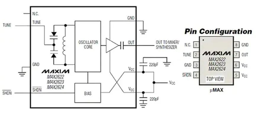
Figure 7: Block diagram and pinout of Maxim Integrated's MAX2623 VCO. The device is a conventional LC-based VCO with voltage control via dual-varactor diodes. The device incorporates an output buffer in its 8-pin package. (Image source: Maxim Integrated)
The design includes an on-chip oscillator inductor and varactor diodes. The device operates from a +2.7 to +5.5V supply and consumes only 8 milliamps (mA). The MAX2623 is one of three VCOs in this product family, and each VCO is different because it has a different expected operating frequency. The MAX2623 has a tuning range of 885 - 950MHz, covering the 902 - 928MHz Industrial, Scientific, and Medical (ISM) frequency band, and can be used as a local oscillator. The VCO delivers an output power level of -3dBm into a 50Ω load with a typical phase noise of -101dBc/Hz at a 100kHz offset. The control voltage range is 0.4 - 2.4V, and the load pull is typically 0.75MHz (pk-pk). The power boost is 280kHz/V (Typ.). Package dimensions are 0.12 x 0.12 x 0.043in. (3.03 x 3.05 x 1.1mm).
Another example of a monolithic VCO is the HMC512LP5ETR from Analog Devices. The VCO has a frequency range of 9.6 - 10.8GHz and a tuning voltage range of 2 - 13V. The device is designed for satellite communications, multipoint radio, and military applications (Figure 8).
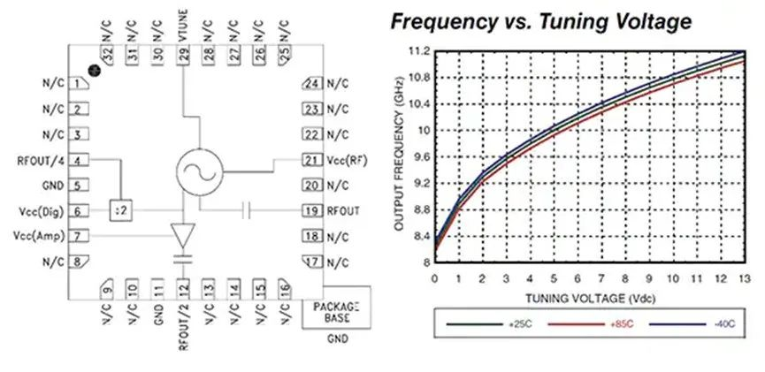
Figure 8: Block diagram of the HMC512LPETR VCO from Analog Devices, showing the integrated varactor diode and oscillator core with an integrated resonator. (Image source: Analog Devices)
This monolithic microwave integrated circuit (MMIC) VCO uses GaAs and InGaP heterojunction bipolar transistors and operates from a 5 V DC supply to achieve wide bandwidth and +9dBm output power level into a 50Ω load. At 100kHz offset, the phase noise is -110dBc/Hz. Load pull is typically 5MHz peak-to-peak (typical). Power boost is typically 30MHz/V (typical) at 5V. The device is packaged in a QFN 5 x 5mm surface mount package. Note that the VCO also includes half and quarter-frequency auxiliary outputs. These fractional frequency outputs can be used to drive a PLL synthesizer to lock to the VCO primary output if required, or to synchronize other timing chain signals.
Small size is both a hallmark and a major advantage of these two monolithic VCO devices.
Ⅷ FAQ about Voltage-Controlled Oscillator
1. What are the advantages of voltage-controlled oscillators?
Advantages are frequency stability with reference to power supply, noise, and temperature, and Accuracy in control of frequency. The main drawback is this type of oscillator cannot be implemented effortlessly on monolithic ICs.
2. What is a voltage-controlled oscillator example?
A practical example of a voltage-controlled oscillator (VCO) is the LM566. The LM566 is a general-purpose VCO that may be used to generate square wave and triangular waveforms as a function input voltage. The LM566 is specified for operation over the 0˚C to 70˚C temperature range.
3. What are the characteristics of VCO?
Characteristics of VCO: (a) Oscillation frequency of voltage-controlled feedback oscillator. (b) The output power of a single oscillator unit with sweeping varactor diode voltage. (c) The closed loop gain of feedback oscillator. (d) Phase noise of feedback oscillator.
4. What is the maximum frequency of VCO?
According to the datasheet, the Maximum frequency of VCO is 24MHz or 38MHz.
5. What is the most common oscillator?
The most common oscillators are the stochastic oscillator, relative strength (RSI), rate of change (ROC), and money flow (MFI).
6. What is the range of VCO?
The oscillation frequency of the designed VCO ranges from 2.42 GHz to 12.12 GHz (S-band to X-band). The 1 MHz offset phase noise of the VCO for an output frequency of 12.12 GHz is found to be -78.87 dBc/Hz without applying any phase noise reduction technique.
 Tesla cuts 10% of global layoffs, Samsung increases NAND flash memory production this quarter4/17/2024 23
1.Tesla announced 10% of its global layoffs, with a higher domestic proportion
Read More > How much do you know about fpga design engineer?4/16/2024 34
Circuitry can be a complex field. The circuit must be completely redone because even the smallest error can drastically alter the project's outcome. One of the numerous individuals involved in circuit building is the FPGA design engineer.An electrical engineer with a focus on designing Field Programmable Gate Array integrated circuits is known as an FPGA engineer.After reading this site, you will be fully informed about fpga design engineers.
Read More > Renesas starts up old factory to increase power device production4/15/2024 20
Renesas Electronics announced in December that the Kofu factory that had previously ceased operations was reactivated. As a 300mm wafer fab, the plant will begin mass production of IGBTs and other products in 2025, doubling Renesas' current power semiconductor production capacity. Renesas held an opening ceremony on April 11, which was attended by local government officials and partner companies.
Read More >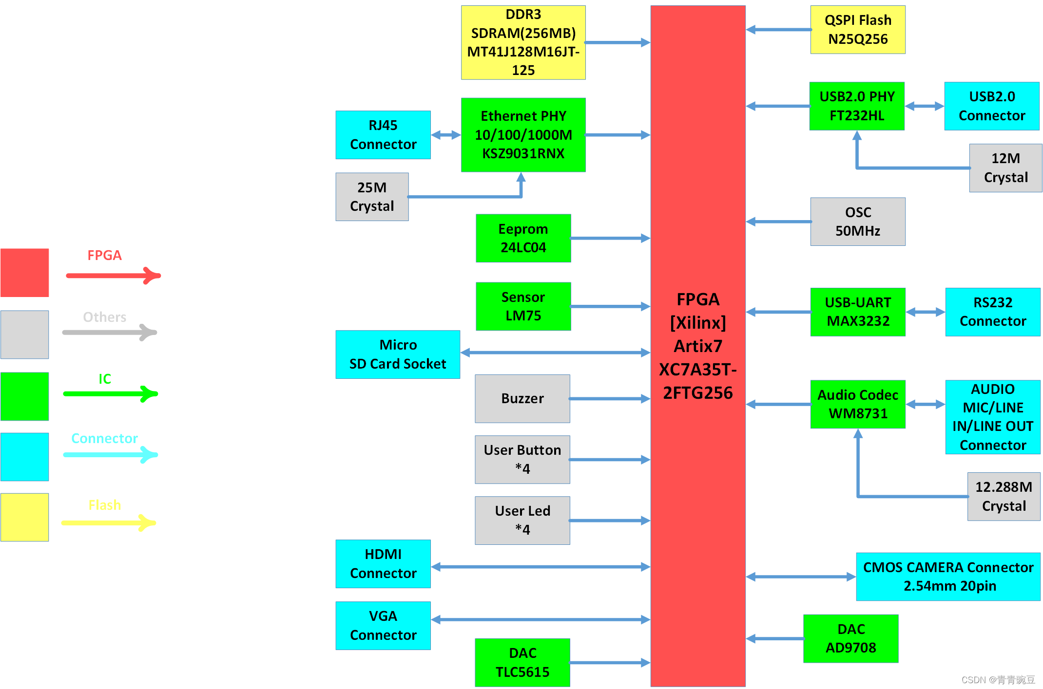 5 key points of Xilinx Artix7 hardware design4/12/2024 32
The following mainly discusses four aspects of the Artix7 chip based on experiences: main chip power supply circuit, selection of main chip filtering capacitors, bank voltage and pin configuration, peripheral circuit construction, and PCB hardware design. These are all summaries obtained after practice, hoping to inspire and help others in their work and study.
Read More > Microchip enabling capacity at TSMC's Kumamoto factory, causing a price increase for Micron products4/11/2024 36
Microchip expands cooperation with TSMC and will establish a 40-nanometer production line at the Kumamoto factory
Read More >
Hot News
- Diode Overview: Application in Automotive Alternator Rectifiers
- Ultra-low power consumption of STM32U575/585 microcontrollers(MCU)
- The Best Guide to Transistor
- Basic Information about Temperature Sensor
- Electronic Component Symbols: Resistor, Capacitor, Transformers and Connectors
- Voltage-Controlled Oscillator: Principle, Type Selection, and Application
SUPPORT
ABOUT BITFOIC
QUICK LINKS
Connect with us
Tel: 86-755-23606554
E-mail: contact@bitfoic.com
Address: Room A29, 24 / F, Hoi Tak Wai, Prince Edward industrial building, 706 Prince Edward Road East, San Po Kong, Kowloon,Hongkong
Mon-Fri: 09.30 AM - 18.30 PM


