


5 key points of Xilinx Artix7 hardware design
Introduction
This blog shares some experiences accumulated in the DIY development of the Artix7 and practical project engineering. Firstly, the Xilinx official hardware design manuals: "ug475_7Series_Pkg_Pinout" and "ug483_7Series_PCB" provide detailed explanations of the pin definitions, power-up sequence, package dimensions, etc., for the entire Xilinx 7 series, including A7, K7, V7, and Spartan7. Secondly, Xilinx has also released some Artix7 development boards such as Nexys, Arty, and Basys3, which offer many details worth referencing. Finally, some development boards from major manufacturers on the market can serve as good references for hardware circuit design, as they have undergone mass production.
The following mainly discusses four aspects of the Artix7 chip based on experiences: main chip power supply circuit, selection of main chip filtering capacitors, bank voltage and pin configuration, peripheral circuit construction, and PCB hardware design. These summaries are obtained after practice, hoping to inspire and help others in their work and study.
Table of Content
Main chip power supply circuit
The power supply chip Artix7 has various voltage types internally, such as VCCO being the reference voltage for the FPGA's IO interface, VCCINT being the core voltage of the FPGA, VCCADC being the supply voltage for the FPGA's internal AD conversion circuit, VCCAUX being the auxiliary voltage of the FPGA, and VCCBRAM being the supply voltage for the FPGA's embedded block RAM. There is a certain power-on sequence requirement here. Generally, the power-on sequence is: 1.0V -> 1.8V -> 1.5V -> 3.3V -> VCCO. Where 1.0V is the voltage for VCCINT and VCCBRAM, 1.8V is for VCCAUX and VCCADC, 1.5V is the reference voltage for external DDR3 memory bank, and 3.3V is the reference voltage for general VCCO bank. This requires multiple DC/DC conversion chips. Therefore, the power supply design of other manufacturers was referenced here, using TLV62130RGT as the onboard DC/DC chip, because this chip itself has EN and PG pins, which enables hardware control of the power-on sequence on the PCB board. The detailed hardware design of the power supply is shown in Figure 1, and the pin power supply voltages for the DIY development board Artix7 chip are shown in Figure 1.
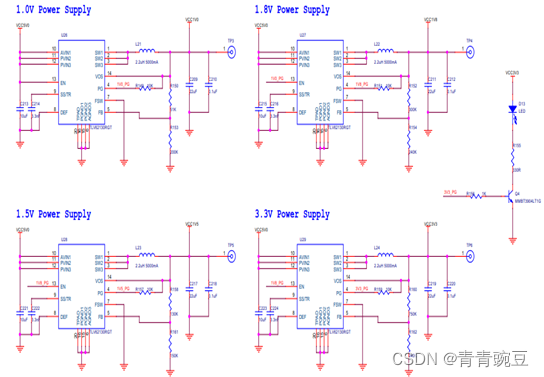
Figure 1 DC/DC power supply circuit of DIY Artix7 development board
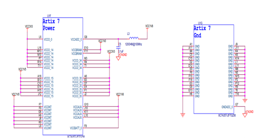
Figure 2 Power supply pins of DIY Artix7 development board
Selection of main chip filter capacitor
When it comes to selecting filtering capacitors, it's essential to read the UG483_7Series_PCB official manual carefully. It provides detailed information on the required capacitance and quantity of filtering capacitors for each FPGA chip of the Xilinx 7 series. The reasonable use and placement of filtering capacitors play a crucial role in ensuring the stable operation of the entire hardware system. I once experimented with other core boards available on the market and encountered hardware instability issues during actual usage. This was largely due to trying to save costs by skimping on filtering capacitors under the FPGA. Therefore, I recommend not compromising hardware stability to save capacitors. This can cause significant headaches during production transitions. Figure 3 shows a screenshot from the UG483_7Series_PCB official hardware design manual. By referencing the XC7A35T-2FTG256C model, you can select the appropriate filtering capacitors for Artix7. While developing this board, there were also some uncertainties regarding minor details. I consulted the official Arty schematic released by Xilinx and the selection of filtering capacitors for the Artix7 DIY development board is illustrated in Figure 3.
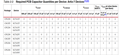
Figure 3 Screenshot of ug483_7Series_PCB official manual
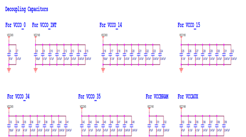
Figure4 Screenshot of ug483_7Series_PCB official manual
Bank voltage and pin configuration
Students who have worked with FPGAs may recall writing XDC constraint files, where different pin voltage definitions are specified, such as LVCMOS33, LVCMOS15, LVTTL, LVDS, and so on. This is related to the voltage supplied to each FPGA bank on the hardware PCB board. For example, let's consider the Pea Development Board with the main control chip XC7A35T-2FTG256C, which contains four banks: Bank14, Bank15, Bank34, and Bank35. The voltage supplied to these banks on the PCB board directly determines the output voltage levels of the IO pins on this bank. For instance, if Bank15 on the development board is connected to a DDR3 chip and requires a supply voltage of 1.5V for its power pins, then the IO pins connected to this bank in the .xdc constraint file need to be defined as LVCMOS15 or LVTTL. Bank14, Bank34, and Bank35 on the PCB board are supplied with a 3.3V reference voltage, so their corresponding IO can be defined as LVCMOS33 or LVTTL. Additionally, in practical project engineering, such as in designing FPGA high-speed interfaces, it's common to need the FPGA's IO to output LVDS voltage levels. In such cases, the corresponding bank's supply pins on the hardware PCB board need to be powered with a voltage of 2.5V.
Regarding this XC7A35T-2FTG256C chip, apart from Bank14, Bank15, Bank34, Bank35, and the power and ground pins, there are some pins used for special functions. In fact, for the Artix7 series chips, these pin names are the same. When drawing the schematic, the author grouped these special pins as shown in Figure 5. This makes it easier for later inspection and maintenance. These pins include JTAG download and debug pins: TDI_0, TDO_0, TCK_0, TMS_0, as well as some other special function pins. The official manual ug475_7Series_Pkg_Pinout also explains whether they need to be pulled up, pulled down, or left unconnected. Here, reference was also made to the development board schematic released by Xilinx, connecting VREFP_0 and VREFN_0 to analog ground, and using a ferrite bead to isolate them from other digital grounds.
One thing to note here is that typically Xilinx FPGA chips will have an external qspi flash connected to store the compiled .mcs program files. The pins connecting this qspi flash to the FPGA chip are fixed. Among them, CCLK_0 needs to be connected to its clock pin, while other pins IO_L1P_T0_D00_MOSI_14, IO_L1N_T0_D01_DIN_14, IO_L2P_T0_D02_14, IO_L2N_T0_D03_14 correspond to DQ0-DQ3 respectively. IO_L6P_T0_FCS_B_14 needs to be connected to the chip select (CS) pin. Here, one can also write FPGA programs to manually control the burning of the .mcs program into this qspi flash through corresponding timing logic, thereby achieving the purpose of remote program updating (about the blog on remote FPGA program updating, the author will write two detailed blogs to describe the design process later). The official document ug470_7Series_FPGAs_Configuration_User_Guide provides detailed interpretations of flash selection, external circuitry, and other configurations.
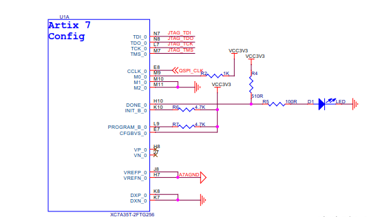
Figure 5 DIY Artix7 development board initialization pin hardware design
Peripheral circuit construction
Through the previous introduction, this XC7A35T-2FTG256C chip has been stable in hardware operation. If it's for an actual project, then we need to select appropriate peripheral circuits according to the project requirements. Let's take an example of an actual engineering project, making a precision instrument, where the control board consists of an STM32 and an Artix7. The Artix7 plays a major role here, including communication with the STM32 via SPI bus, real-time sampling and calculation of voltage and current RMS, average, peak values from the backend ADC, performing FFT on the sampled points to restore their input waveform and pack them for output to the STM32, responding to setting DAC commands from the STM32 including voltage, current, frequency waveform, etc., then outputting through a DDS signal generator. It's externally connected to USB 2.0 and RS232 interfaces. These interfaces can input special waveform shapes through a host computer, the FPGA reads these points and writes them into EEPROM, so that after power loss, the STM32 can directly control and output the specified frequency waveform shape set by the host computer. So, considering this actual project, the XC7A35T-2FTG256C chip should be connected to the STM32 via an SPI bus, and hardware-wise connected to the backend ADC analog-to-digital, DAC digital-to-analog chips. An I2C bus connects to EEPROM, and additionally, hardware connections are needed to the external USB 2.0 interface chip FT232HL, and RS232 interface chip MAX3232, for host computer communication.
As shown in Figure 6, the overall design architecture of the DIY Artix7 development board schematic, the author integrates many commonly used modules such as temperature sensors, EEPROM, buttons, indicators, SD cards, buzzers, etc., on this development board according to work and study needs. Simultaneously, the development board also includes common external interfaces such as USB 2.0, Gigabit Ethernet port, and RS232 serial port. The board is equipped with DDR3 memory chips for easy storage and processing of large amounts of data, and QSPI flash for power-off storage of .mcs files. Additionally, the development board includes a serial DAC, and a parallel DAC, facilitating early-stage verification of complex digital signal processing. The VGA and HDMI, CMOS camera interfaces also allow this development board to perform image and video processing experiments well. Finally, with an audio codec chip WM8731, in leisure time, you can also research audio signal input and output.
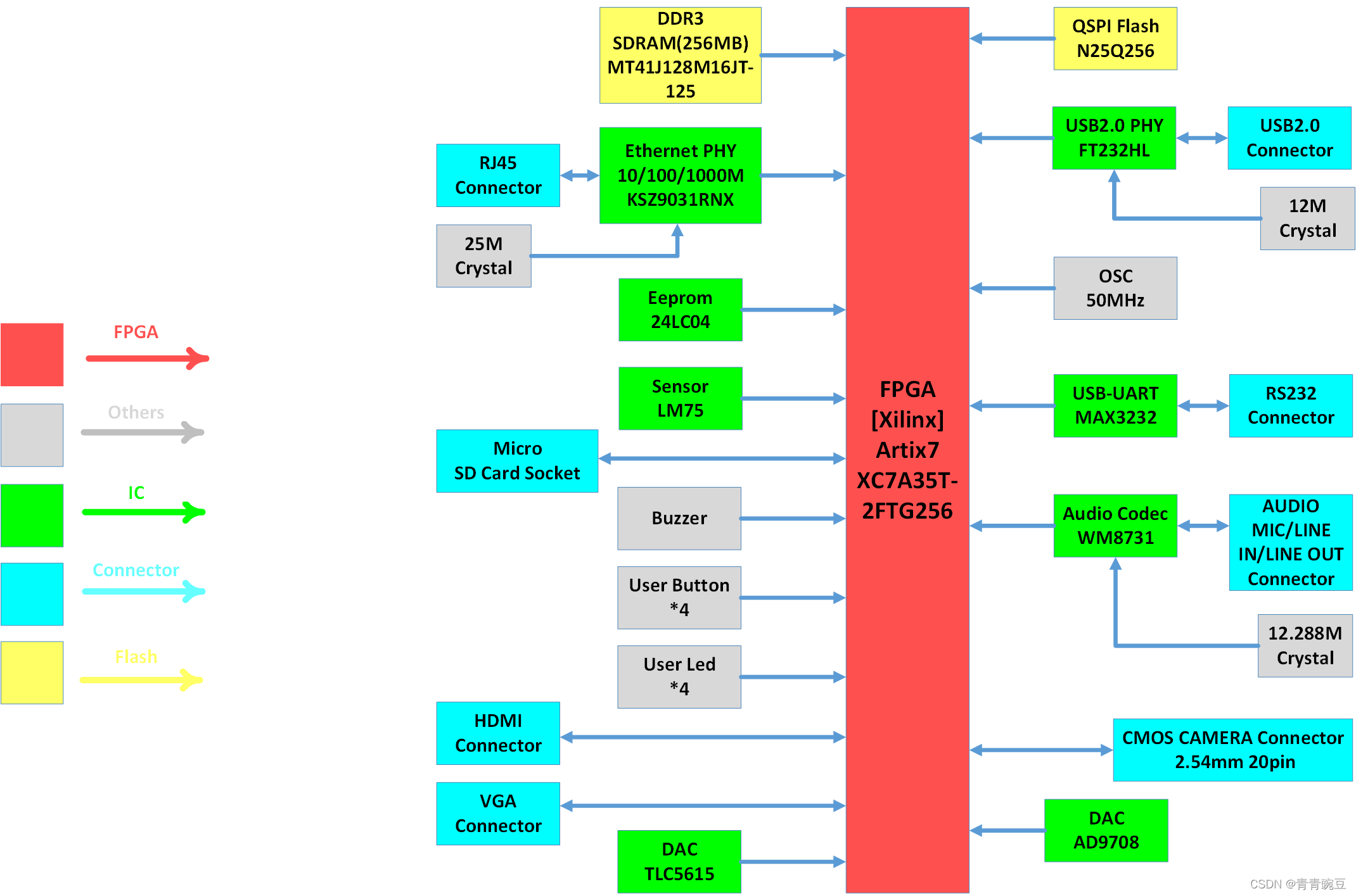
Figure 6 DIY Artix7 development board schematic diagram overall design architecture
PCB board hardware design
After the preceding requirements analysis, schematic design, and component library creation, we now move on to the stage of PCB layout design. In reality, many FPGA engineers or hardware engineers tend to overlook PCB layout design, not delving deeply into it. Some may even think that just connecting the traces is sufficient, and if it doesn't work, adding more layers will solve the issue. However, PCB layout design plays a crucial role in the entire hardware design process, directly determining the performance of the PCB. Figures 12 to 15 respectively depict the top layer, ground layer, power layer, and bottom layer PCB layout designs of the DIY Artix7 development board. Since the IO ports of FPGA themselves possess strong reusability, adjustments in routing and modifications in the schematic can be made during PCB design to ensure smooth routing to the greatest extent possible, thereby facilitating layout wiring and also reducing the number of PCB layers, significantly reducing costs.
A four-layer PCB board design was adopted in designing this DIY development board, considering that the main chip XC7A35T-2FTG256C only has 256 pins. The entire development board maintains 50-ohm impedance matching for routing and 100-ohm impedance matching for differential signals. Core modules such as DDR3 are designed with equal-length traces, with signal lines grouped and routed on the same layer strictly following specifications in the PCB layout design. Additionally, good separation between analog ground and digital ground layers, as well as power layers, has been ensured. This guarantees that the top and bottom layer routing will have excellent reference planes. The layout of the entire development board is neat, and aesthetically pleasing, with good performance and clear silkscreen markings. Finally, considering the high line density, during actual routing, a 5-mil line width was used for single traces, and the spacing between differential traces was adjusted.
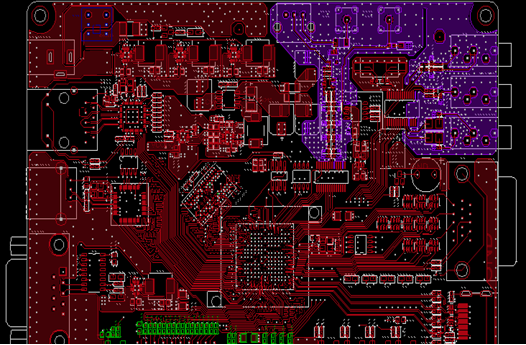
Figure 7 DIY Artix7 development board top-level PCB file
 Tesla cuts 10% of global layoffs, Samsung increases NAND flash memory production this quarter4/17/2024 25
1.Tesla announced 10% of its global layoffs, with a higher domestic proportion
Read More > How much do you know about fpga design engineer?4/16/2024 41
Circuitry can be a complex field. The circuit must be completely redone because even the smallest error can drastically alter the project's outcome. One of the numerous individuals involved in circuit building is the FPGA design engineer.An electrical engineer with a focus on designing Field Programmable Gate Array integrated circuits is known as an FPGA engineer.After reading this site, you will be fully informed about fpga design engineers.
Read More > Renesas starts up old factory to increase power device production4/15/2024 27
Renesas Electronics announced in December that the Kofu factory that had previously ceased operations was reactivated. As a 300mm wafer fab, the plant will begin mass production of IGBTs and other products in 2025, doubling Renesas' current power semiconductor production capacity. Renesas held an opening ceremony on April 11, which was attended by local government officials and partner companies.
Read More > Microchip enabling capacity at TSMC's Kumamoto factory, causing a price increase for Micron products4/11/2024 42
Microchip expands cooperation with TSMC and will establish a 40-nanometer production line at the Kumamoto factory
Read More >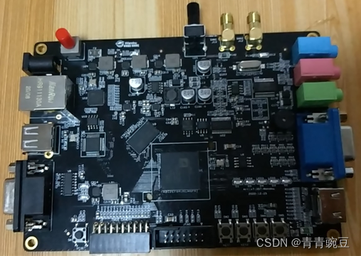 How to Design PCB Based on Xilinx Artix7?4/10/2024 41
When it comes to PCB hardware design, everyone understands that you need to start with schematic design, then create component footprints, followed by layout and routing, and finally, after soldering the board, you come back for debugging.
Read More >
Hot News
- Diode Overview: Application in Automotive Alternator Rectifiers
- Ultra-low power consumption of STM32U575/585 microcontrollers(MCU)
- The Best Guide to Transistor
- Basic Information about Temperature Sensor
- Electronic Component Symbols: Resistor, Capacitor, Transformers and Connectors
- Voltage-Controlled Oscillator: Principle, Type Selection, and Application
SUPPORT
ABOUT BITFOIC
QUICK LINKS
Connect with us
Tel: 86-755-23606554
E-mail: contact@bitfoic.com
Address: Room A29, 24 / F, Hoi Tak Wai, Prince Edward industrial building, 706 Prince Edward Road East, San Po Kong, Kowloon,Hongkong
Mon-Fri: 09.30 AM - 18.30 PM


