


STM32 devices will break through 20nm
- SEMI: Multiple applications promote the expansion of investment scale in 300 mm wafer fabs
According to a report released by the International Semiconductor Industry Association (SEMI), global spending on 300mm fab equipment for front-end facilities will increase by 20% in 2025, reaching 116.5 billion due to the recovery of the memory market and strong demand for high-performance computing and automotive applications. The U.S. dollar will grow by 12% in 2026 to reach $130.5 billion and will hit a record high of $137 billion in 2027.

source: SEMI
By region, mainland China will invest US$30 billion annually in the next four years and continue to lead fab equipment spending. Taiwan, South Korea, and the United States follow. By field, wafer manufacturing will grow at a compound growth rate of 7.6% to US$79.1 billion in 2027, followed by memory, analog, optoelectronics, and discrete devices.
- ST releases ultra-low power controller STM32U0 series
STMicroelectronics (ST) released the ultra-low-power microcontroller (MCU) STM32U0 series on the 19th. The new products will be combined with ST’s most advanced design technology and advanced manufacturing processes to achieve a huge leap in energy efficiency. This MCU reduces energy consumption by 50% compared to previous generations.
STM32U0 has many analog peripherals, such as ADC and DAC) operational amplifiers and comparators. There is also an on-chip system oscillator that helps reduce the bill of materials, saving cost and PCB space. The product suits industrial, medical, smart metering, and consumer applications. The STM32U0 series is in mass production, with prices starting at US$0.68 for 1,000 pieces.
- ST will introduce processes within 20nm for the next-generation MCU to improve several key performance
STMicroelectronics (ST) announced on the 19th that the first STM32 microcontroller (MCU) based on new technology will be sampled for selected customers in the second half of 2024. The 18nm FD-SOI process and embedded phase change memory (PCM) will achieve a leap in performance and power consumption.
This new process technology, jointly developed by ST and Samsung Foundry, brings a leap in performance and power consumption for embedded processing applications while allowing for larger memory sizes and higher levels of simulation and Digital peripheral integration. Based on the new technology, the first next-generation STM32 microcontrollers will begin sampling to selected customers in the second half of 2024, with production planned for the second half of 2025.
- TSMC and Synopsys will use the NVIDIA computational lithography platform
NVIDIA recently announced at the annual GTC conference in San Jose, California, that to speed up the manufacturing of next-generation advanced semiconductor chips and overcome physical limitations, TSMC and Synopsys will use the NVIDIA computational lithography platform in production.
TSMC, the world's leading foundry, and Synopsys, a leader in wafer-to-system design solutions, have integrated NVIDIA cuLitho into their software, manufacturing processes, and systems to accelerate chip manufacturing while also accelerating their vision for the future. Support for the latest generation of NVIDIA Blackwell architecture GPUs.
Currently, many changes in fab processes require modifications to OPC, which increases the amount of calculations and creates a bottleneck in the fab development cycle. With the accelerated computing and generative AI provided by cuLitho, these costs and bottlenecks can be alleviated, allowing fabs to design more novel solutions when developing new technologies at 2nm and beyond.
5. NXP cooperates with NVIDIA to deploy AI models on edge device combinations
NXP recently announced that it will enable NVIDIA’s trained artificial intelligence models to be deployed on NXP’s broad portfolio of edge processing devices through the eIQ machine learning development environment. It will integrate NVIDIA TAO toolkit functions into NXP’s eIQ machine learning development environment to gain The ability to accelerate development. NXP is the first semiconductor vendor to integrate the NVIDIA TAO API directly into its AI-enabled products, making it easier for developers to deploy trained AI models at the edge.
The NXP eIQ machine learning software development environment allows the use of artificial intelligence algorithms across NXP’s broad portfolio of microcontrollers and microprocessors. It is fully integrated into NXP's MCUXpresso SDK and Yocto Project Linux development environment, allowing developers to develop complete system-level applications easily.
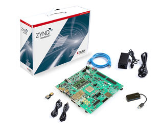 ZCU106 Evaluation Kit: Overview, Features,Components, Quick start guide5/10/2024 7
The ZCU106 Evaluation Kit is a development board designed by Xilinx for prototyping and evaluating designs based on their Zynq UltraScale+ MPSoC platform. This guide will provide an overview of the kit, its components, and how to get started with it.
Read More > Infineon's profit decreases, memory Q2 contract price increase revised upwards5/9/2024 23
Infineon recently announced its results for the second quarter of fiscal year 2024. Revenue was 3.632 billion euros, down 12% year-on-year and 2% month-on-month; profit was 707 million euros, down 40% year-on-year and 15% month-on-month; gross profit margin was 38.6%. , a year-on-year decrease of 8 percentage points and a month-on-month decrease of 4.6 percentage points.
Read More >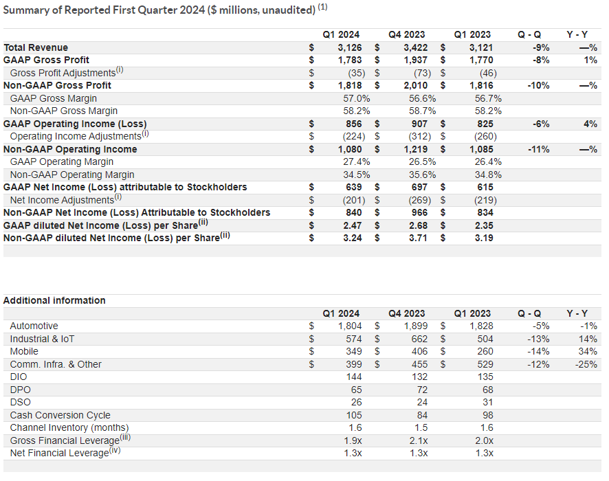 NXP and ON Semiconductor released financial reports5/5/2024 30
NXP and ON Semiconductor released financial reports, rising copper prices were transmitted to the IC industry
Read More > Tesla cuts 10% of global layoffs, Samsung increases NAND flash memory production this quarter4/17/2024 29
1.Tesla announced 10% of its global layoffs, with a higher domestic proportion
Read More > How much do you know about fpga design engineer?4/16/2024 58
Circuitry can be a complex field. The circuit must be completely redone because even the smallest error can drastically alter the project's outcome. One of the numerous individuals involved in circuit building is the FPGA design engineer.An electrical engineer with a focus on designing Field Programmable Gate Array integrated circuits is known as an FPGA engineer.After reading this site, you will be fully informed about fpga design engineers.
Read More >
Hot News
- Diode Overview: Application in Automotive Alternator Rectifiers
- Ultra-low power consumption of STM32U575/585 microcontrollers(MCU)
- The Best Guide to Transistor
- Basic Information about Temperature Sensor
- Electronic Component Symbols: Resistor, Capacitor, Transformers and Connectors
- Voltage-Controlled Oscillator: Principle, Type Selection, and Application
SUPPORT
ABOUT BITFOIC
QUICK LINKS
Connect with us
Tel: 86-755-23606554
E-mail: [email protected]
Address: Room A29, 24 / F, Hoi Tak Wai, Prince Edward industrial building, 706 Prince Edward Road East, San Po Kong, Kowloon,Hongkong
Mon-Fri: 09.30 AM - 18.30 PM


