


How to Design PCB Based on Xilinx Artix7?
Introduction
When it comes to PCB hardware design, everyone understands that you need to start with schematic design, then create component footprints, followed by layout and routing, and finally, after soldering the board, you come back for debugging. In actual work, going through this process gives you a general understanding of PCB design. Of course, selecting components, reading datasheets, circuit construction, power supply design, layout, routing, etc., each of these aspects is substantial enough to fill a thick book. So here, let's briefly discuss PCB design in practical project engineering and how to make our boards exquisite, beautiful, robust, and durable.
This blog mainly summarizes some PCB design knowledge accumulated in the work and the key points of Xilinx Artix7 hardware design. I draw a development board welding proof and expand the required hardware resources together as shown in Figure 1.
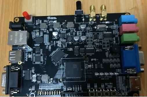
Figure 1 development board
How to Choose a SOC chip?
Embedded products usually require consideration of many aspects on the hardware side, but cost after batch PCB production is an inevitable topic. This involves the selection of SOC chips, PCB layering design, peripheral circuit construction, and more.
Let's take a real engineering example: the front display board of a device. Suppose the main chip selected is STM32F429 for driving. In that case, an external SDRAM is needed to cache images for the display screen because it needs to run ST's official Emwin and other human-machine interface graphics libraries. An external flash is required to store these images to display boot logos and other icons on the interface. Additionally, certain parameters need to be preserved during power-off on the display panel, so an external EEPROM is needed, and then the software needs to be developed according to the onboard hardware platform.
In practical projects, consumer-grade PCB boards typically consider economic factors, with 4 or 6 layers being the most common. For military-grade applications, more emphasis is placed on performance indicators, often leading to the choice of 8 layers or more. Components chosen for military-grade applications also tend to offer higher stability compared to those for consumer-grade applications.
Generally, a 4-layer PCB board is sufficient to meet the requirements of the vast majority of consumer-grade products. Compared to 2-layer boards, 4-layer PCB designs offer more room for flexibility and have a slightly higher price. They also allow for easier impedance matching by providing additional reference planes, facilitating longer designs, and so on.
For standard 4-layer boards, the single-line width is typically 6 mils, the differential pair trace width is 4.9 mils, and the differential pair spacing is 7.8 mils. Internal lines should maintain an equal length of 5-10 mils. If higher line density requires reducing trace widths, adjusting the board thickness can achieve this. For example, in a DIY Artix7 development board, single-line width could be adjusted to 5 mils, with a differential pair trace width of 4.9 mils and a spacing of 8.2 mils.
The number of layers in a PCB is often determined by the main system-on-chip (SOC) component. For instance, selecting a QFP package or a BGA package with only 256 pins can usually be accommodated with a 4-layer board, even if the board includes DDR3 or SDRAM chips. However, choosing a BGA package with 484 pins typically requires a 6-layer board or even more layers.
Before selecting the main SOC chip, it's crucial to clearly define the functional requirements. You can refer to the official chip manual extensively. Choose one that is available and also offers the best cost-performance ratio. At this point, we should pay more attention to whether there are any special considerations. For example, some SOC chips require different types of voltage supply to function properly, and there may be requirements regarding the power-on sequence between these voltages. Another consideration is when evaluating requirements for external memory expansion, such as needing to attach four DDR3 chips as external memory for the SOC chip. Some SOC chip manuals explicitly state that they do not support fly-by topology, only T topology.
Additionally, in a project requiring multiple UART and SPI interfaces, it's important to check if the selected SOC chip has sufficient pins. If not, can pin multiplexing be done? Are there multiple DMA channels available for convenient programming? If there are uncertainties, it's advisable to refer to the official manuals as well as mature development board designs on the market.
When initially designing this DIY Artix7 development board, there were uncertainties about the power-on sequence for the Artix7 chip's banks and the selection of filter capacitors for the Artix7 chip. The author repeatedly verified the Xilinx official hardware design manual and Xilinx official development boards. After PCB assembly and soldering, debugging was done gradually until stability was achieved.
Therefore, it is recommended that friends pay attention to both embedded software and hardware aspects, as well as the overall product architecture. It's beneficial to explore peripheral knowledge, which is very helpful for everyone's future development. For example, if one becomes proficient in FPGA and also masters knowledge related to medical devices or power electronics, prospects will be promising, and with accumulated project experience, there will be low substitutability.
How to Choose Xilinx Artix7?
The DIY development board integrates a Xilinx A7 series chip as its main controller, with the classic model being XC7A35T-2FTG256C. Some might wonder why this chip was chosen over others like Spartan7, K7, or V7 from the Xilinx 7 series. Figure 2 in the Xilinx official manual showcases the promotional illustration of the 7 series chips.
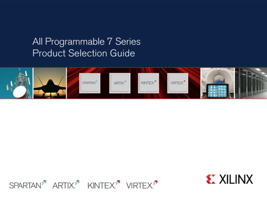
Figure 2 Promotional poster for Xilinx 7 series chips
Through repeated study of the Xilinx 7 series chip manual, although there are many types of Xilinx chips, from a research and development perspective, I believe that there are two chips from Xilinx that stand out: the Spartan-6XC6SLX9 and the XC7A35T-2FTG256C. These can be considered the kings of cost-effectiveness. Below, I will briefly analyze the selection of Xilinx chips.
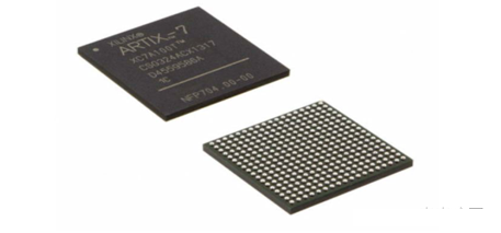
Figure3-Xilinx 7 series
Once accustomed to using Spartan6, one might think it's time to follow in the footsteps of Spartan7. However, Spartan7, compared to A7, K7, and V7, was launched later, meaning it's more innovative. However, its resources are not significantly different from A7, yet its price remains high due to supply issues. In contrast, the A7 has been stable in supply for many years, thoroughly tested by the market, and offers a variety of models to meet different customer needs.
From a practical R&D perspective, there are two notable aspects where A7 shines. Firstly, although all A7 models come in BGA packages, they offer options like 256PIN, 325PIN, 484PIN, 676PIN, etc., allowing customers to choose according to their needs. For typical projects, an A7 256PIN four-layer board is usually sufficient, and then it can be evaluated whether external SDRAM or DDR3 memory chips are needed, as well as the required resource size—be it 35T, 50T, or 100T, etc. If there's a need for two external DDR3 memory chips, one can consider whether the 484PIN model meets the requirements in terms of pin availability and allocation.
Secondly, regardless of the resource size—whether it's 35T, 50T, 100T, or 200T—A7 series models with 484PIN have identical pin definitions and chip packaging, ensuring maximum hardware compatibility. The naming conventions for the Artix7 series are illustrated in Figure 4.
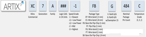
Figure 4 Schematic diagram of Xilinx Artix7 chip naming rules
The resource situation of various models of Artix7 is shown in Figure 5. Here, friends can use Vivado-generated resource reports to estimate the appropriate chip model for their project engineering. Of course, in actual projects, there is a great deal of flexibility to analyze specific situations. For example, some resources can be substituted, and RAM and FIFO are widely used in FPGA designs. In Xilinx's Vivado environment, different resources can be used to generate RAM and FIFO, either using LUTs or Block RAM.
For instance, in digital signal processing, FFT operations and other IP cores offer the option of serial or parallel computation configurations. If strict time requirements are not necessary, configuring them as serial can save resources. Additionally, in image and video development, if the onboard only has two DDR3 chips, it's clear that the read/write speed is not as convenient as having four DDR3 chips. To balance hardware costs and user experience, caching three frames of image processing can be a compromise. This approach has been proven effective in practical applications.
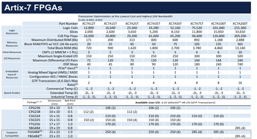
Figure 5 The number of resource logic of each model of Xilinx Artix7 chip
In summary, everyone needs to choose the chip according to the actual situation of their project. The next article will share key points of Xilinx Artix7 hardware design that you may find interesting.
 ZCU106 Evaluation Kit: Overview, Features,Components, Quick start guide5/10/2024 2
The ZCU106 Evaluation Kit is a development board designed by Xilinx for prototyping and evaluating designs based on their Zynq UltraScale+ MPSoC platform. This guide will provide an overview of the kit, its components, and how to get started with it.
Read More > Infineon's profit decreases, memory Q2 contract price increase revised upwards5/9/2024 11
Infineon recently announced its results for the second quarter of fiscal year 2024. Revenue was 3.632 billion euros, down 12% year-on-year and 2% month-on-month; profit was 707 million euros, down 40% year-on-year and 15% month-on-month; gross profit margin was 38.6%. , a year-on-year decrease of 8 percentage points and a month-on-month decrease of 4.6 percentage points.
Read More > NXP and ON Semiconductor released financial reports5/5/2024 26
NXP and ON Semiconductor released financial reports, rising copper prices were transmitted to the IC industry
Read More > Tesla cuts 10% of global layoffs, Samsung increases NAND flash memory production this quarter4/17/2024 28
1.Tesla announced 10% of its global layoffs, with a higher domestic proportion
Read More > How much do you know about fpga design engineer?4/16/2024 54
Circuitry can be a complex field. The circuit must be completely redone because even the smallest error can drastically alter the project's outcome. One of the numerous individuals involved in circuit building is the FPGA design engineer.An electrical engineer with a focus on designing Field Programmable Gate Array integrated circuits is known as an FPGA engineer.After reading this site, you will be fully informed about fpga design engineers.
Read More >
Hot News
- Diode Overview: Application in Automotive Alternator Rectifiers
- Ultra-low power consumption of STM32U575/585 microcontrollers(MCU)
- The Best Guide to Transistor
- Basic Information about Temperature Sensor
- Voltage-Controlled Oscillator: Principle, Type Selection, and Application
- Electronic Component Symbols: Resistor, Capacitor, Transformers and Connectors
SUPPORT
ABOUT BITFOIC
QUICK LINKS
Connect with us
Tel: 86-755-23606554
E-mail: [email protected]
Address: Room A29, 24 / F, Hoi Tak Wai, Prince Edward industrial building, 706 Prince Edward Road East, San Po Kong, Kowloon,Hongkong
Mon-Fri: 09.30 AM - 18.30 PM


