


An introduction to Xilinx XC9572XL Series FPGA
Introduction
A CPLD called the Xilinx XC9572XL was created especially for high-performance, low-voltage applications in computer and telecommunication systems. It also consists of four 54V18 Function Blocks with 1,600 useable gates each. The Xilinx FPGA XC9572XL has a high I/O per macrocell count and several sophisticated system features.
Additionally, this device fits neatly into the current design flow. As a result, this facilitates time savings and simplifies design. Stealing saved designs is not possible with the Xilinx XC9572XL. This gadget has enhanced security. It can also be reprogrammed to address any system errors.
Table of Content
What is XC9572XL?
The Xilinx XC9572XL has pin-to-pin logic delays of 5 ns. This device's system frequency is also approximately 178 MHz. 1,600 useable gates are available across 72 macrocells in the Xilinx XC9572XL design. This gadget is designed to operate at peak efficiency on 3.3V systems. It thereby provides Fast FLASHTM technology and low-power operation.
Xilinx XC9572XL fully supports IEEE standard 1149.1 boundary-scan (JTAG). This makes it possible to create and debug small-footprint packages more effectively. Additionally, each macrocell may operate on minimal power thanks to this device. Consequently, this makes it possible to reduce gadget power drastically. The user can set each macrocell to operate in low power mode.
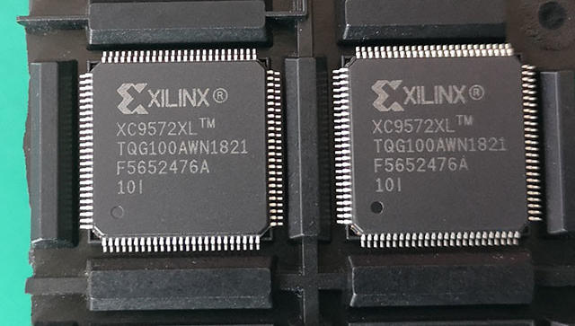
Figure1-XC9572XL family
To be compatible with Spartan-XL and Xilinx Virtex, the Xilinx XC9572XL family was created specifically. As a result, this gives system designers the best possible separation of logic between quick interface circuitry and high-density general-purpose logic. The XC9572XL series is pin-compatible as well. This facilitates the migration of design across many density possibilities within a given package footprint.
The XC9572XL device has multiple function blocks and I/O blocks. It is a subsystem, this gadget. Buffering for device outputs and inputs is provided via the I/O block. Every functional block (FB) can use programmable logic. Furthermore connecting all input signals and FB outputs to the FB inputs is the FastCONNECT II switch matrix.
XC9572XL Features
- 5 ns pin-to-pin logic delays
- System frequency up to 178 MHz
- 72 macrocells with 1,600 usable gates
- Available in small-footprint packages
- 44-pin PLCC (34 user I/O pins)
- 44-pin VQFP (34 user I/O pins)
- 48-pin CSP (38 user I/O pins)
- 64-pin VQFP (52 user I/O pins)
- 100-pin TQFP (72 user I/O pins)
- Pb-free available for all packages
- Optimized for high-performance 3.3V systems
- Low power operation
- 5V tolerant I/O pins accept 5V, 3.3V, and 2.5V signals
- 3.3V or 2.5V output capability
- Advanced 0.35-micron feature size CMOS Fast FLASH™ technology
- Advanced system features
- In-system programmable
- Superior pin-locking and routability with Fast CONNECT™ II switch matrix - Extra wide 54-input Function Blocks
- Up to 90 product terms per macrocell with individual product-term allocation
- Local clock inversion with three global and one product-term clocks
- Individual output enable per output pin
- Input hysteresis on all user and boundary-scan pin inputs
- Bus-hold circuitry on all user pin inputs
- Full IEEE Standard 1149.1 boundary scan (JTAG)
- Fast concurrent programming
- Slew rate control on individual outputs
- Enhanced data security features
- Excellent quality and reliability
- Endurance exceeding 10,000 program/erase cycles - 20-year data retention - ESD protection exceeding 2,000
- Pin-compatible with 5V-core XC9572 device in the 44-pin PLCC package and the 100-pin TQFP package
WARNING: Programming temperature range of TA = 0° C to +70° C
XC9572XL Benefits
Fast concurrent programming
Excellent reliability and endurance
Improved design security
5V tolerant I/Os
Optimized for high-performance 3.3V systems
Small footprint packages
How to minimize power dissipation in Xilinx XC9572XL CPLD?
Power dissipation in CPLDs can vary significantly depending on the output loading and system frequency. Design applications can also determine power dissipation. Each macrocell in the Xilinx XC9572XL CPLD can be set up to operate in low power mode. In doing so, power dissipation is reduced. Moreover, macrocells and unused product keywords are immediately deactivated by the software. As a result, this promotes energy conservation.
You can use the following equation for an estimate of Icc.
ICC(mA) = MCHS(0.175*PTHS + 0.345) + MCLP(0.052*PTLP + 0.272) + 0.04 * MCTOG(MCHS +MC)
Here:
- The term "MCHS" describes the high-speed configuration of macrocells.
- The macrocells in low power configuration, or MCLP for short,
- f refers to the maximum clock frequency
- PTLP refers to the average number of low-power product terms for each macrocell
- PTHS refers to the average number of high-speed product terms for each macrocell
- MCTOG refers to the average % of flip-flops per clock
The Architectural Description of XC9572XL
Several units make up the Xilinx XC9572XL.
Function block (FB)
Each function block is made up of separate macrocells. Global clock, reset/set, and output enable signals are also received by the function block. The outputs generated by this block support the FastCONNECT switch matrix. Using a sum-of-products representation facilitates the application of FB's logic.
Macrocell
It is possible to individually configure each macrocell in XC9572XL for a combinatorial or registered function. The macrocell register can be set up as a D-type or T-type flip-flop. Additionally, it is avoidable for combinatorial operations. Set and reset operations can be performed asynchronously on any register.
FastCONNECT II switch matrix
Signals are connected to the function block inputs in this way. This matrix is driven by all of the functional block and I/O block outputs.
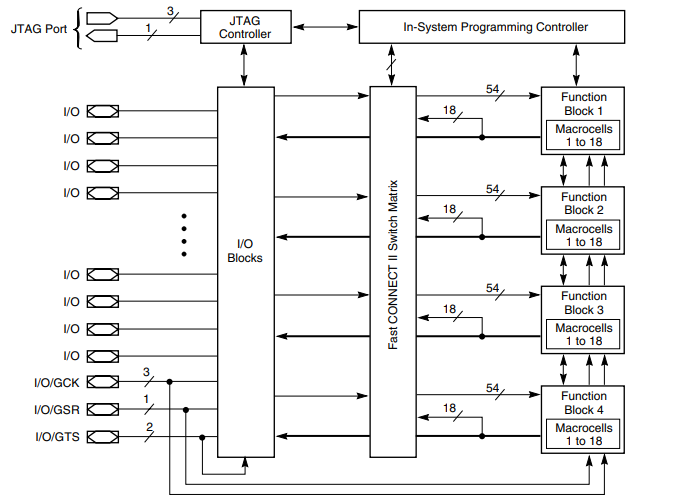
Figure 2: XC9572XL Architecture
Input/output block
The I/O Block, also called the IOB, serves as an interface between internal logic and the device's user I/O pins. An output driver and an output enable selection multiplexer are included with each IOB. Additionally, each IOB has an input buffer and user-programmable ground control.
User-programmable ground pin capability is available on all IOBs. Consequently, you can set up device I/O pins as extra ground pins thanks to this. Unused pins will be forced to a low-voltage state as a result. Every I/O block has bus-hold circuitry that is always operational when there is legitimate user activity. Furthermore, there's no need to bind unneeded pins high or low because of the bus-hold property.
Every output driver has the option to be configured for slew-rate limited operation. All output drivers are capable of providing low-power noise and quick switching. Grounding capability may be present in all output drivers. This is something internal logic can accomplish. An essential component of the FPGA of the Xilinx XC9572XL series is the IOB.
Xilinx XC9572XL Devices recommend
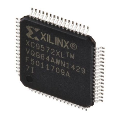
Figure3-XC9572XL-7VQG64I
XC9572XL-7VQG64I is a complex programmable logic device (CPLD) launched by Xilinx. CPLD is a digital circuit device with high flexibility and programmability and is widely used in electronic equipment in various fields.
One of the features of the XC9572XL-7VQG64I is its high logic density and large memory capacity. It uses advanced CMOS technology, has 72 macro cells and 5,760 available logic cells, and can implement complex logic functions. In addition, it comes with a 64-pin package for easy connection with other electronic components.
The XC9572XL-7VQG64I also features low power consumption and high performance. It uses dynamic power management technology to reduce power consumption as much as possible while meeting design requirements. At the same time, it supports fast clock frequencies and has fast output drive capabilities, making it excellent in high-speed applications.
In addition to this, the XC9572XL-7VQG64I also has programmable input/output pins that can be configured according to specific design needs. It supports a variety of common digital logic standards, such as TTL, CMOS, and LVCMOS, and also provides rich clock management functions, including frequency division, frequency multiplication, and phase locking.
The development tools and software ecosystem of the XC9572XL-7VQG64I are also very complete. Xilinx provides a powerful and easy-to-use development tool suite, including design software, simulation tools, and debuggers, to facilitate developers to design and verify hardware. In addition, Xilinx also provides a wealth of technical documentation and sample code to help users get started quickly and achieve their design goals.
In short, the XC9572XL-7VQG64I is a complex programmable logic device with powerful functions and high flexibility. It plays an important role in various applications, providing reliable and efficient digital logic control capabilities for electronic devices.
 ZCU106 Evaluation Kit: Overview, Features,Components, Quick start guide5/10/2024 2
The ZCU106 Evaluation Kit is a development board designed by Xilinx for prototyping and evaluating designs based on their Zynq UltraScale+ MPSoC platform. This guide will provide an overview of the kit, its components, and how to get started with it.
Read More > Infineon's profit decreases, memory Q2 contract price increase revised upwards5/9/2024 11
Infineon recently announced its results for the second quarter of fiscal year 2024. Revenue was 3.632 billion euros, down 12% year-on-year and 2% month-on-month; profit was 707 million euros, down 40% year-on-year and 15% month-on-month; gross profit margin was 38.6%. , a year-on-year decrease of 8 percentage points and a month-on-month decrease of 4.6 percentage points.
Read More > NXP and ON Semiconductor released financial reports5/5/2024 26
NXP and ON Semiconductor released financial reports, rising copper prices were transmitted to the IC industry
Read More > Tesla cuts 10% of global layoffs, Samsung increases NAND flash memory production this quarter4/17/2024 28
1.Tesla announced 10% of its global layoffs, with a higher domestic proportion
Read More > How much do you know about fpga design engineer?4/16/2024 54
Circuitry can be a complex field. The circuit must be completely redone because even the smallest error can drastically alter the project's outcome. One of the numerous individuals involved in circuit building is the FPGA design engineer.An electrical engineer with a focus on designing Field Programmable Gate Array integrated circuits is known as an FPGA engineer.After reading this site, you will be fully informed about fpga design engineers.
Read More >
Hot News
- Diode Overview: Application in Automotive Alternator Rectifiers
- Ultra-low power consumption of STM32U575/585 microcontrollers(MCU)
- The Best Guide to Transistor
- Basic Information about Temperature Sensor
- Voltage-Controlled Oscillator: Principle, Type Selection, and Application
- Electronic Component Symbols: Resistor, Capacitor, Transformers and Connectors
SUPPORT
ABOUT BITFOIC
QUICK LINKS
Connect with us
Tel: 86-755-23606554
E-mail: [email protected]
Address: Room A29, 24 / F, Hoi Tak Wai, Prince Edward industrial building, 706 Prince Edward Road East, San Po Kong, Kowloon,Hongkong
Mon-Fri: 09.30 AM - 18.30 PM


