


VCU118 Evaluation Board: User Guide,Block Diagram and Features
Introduction
Engineers and developers wishing to investigate the possibilities of FPGA technology will find the VCU118 evaluation board to be a strong and adaptable instrument. Thanks to its versatile interface options and strong processing capabilities, the board is well-suited to various applications, from digital signal processing and machine learning to image and video processing. Any developer can benefit greatly from the VCU118 board, whether they're trying to push the limits of FPGA technology or prototype a new application.
Table of Content
VCU118 Product Description
The AMD Virtex UltraScale+ FPGA VCU118 evaluation kit is called EK-U1-VCU118-G. It is the perfect setting for development to assess the state-of-the-art Virtex UltraScale+ FPGAs. The highest performance and integration capabilities in a FinFET node are offered by Virtex UltraScale+ devices, which also have the largest on-chip memory density and serial I/O and signal processing bandwidth. This kit is perfect for prototyping applications, from 1+ Tb/s networking and data centers to fully integrated radar/early-warning systems.
From fully integrated radar/early-warning systems to networking and data centers with throughputs of 1+ Tb/s, this kit is perfect for prototyping applications.
Ultimately, the VCU118 evaluation board offers a strong and adaptable platform for creating and testing sophisticated digital ideas. Thanks to its many interfaces, high-speed processing capabilities, and abundant programmable logic, it may be used for many different tasks, including machine learning, high-performance computing, networking, and video processing.
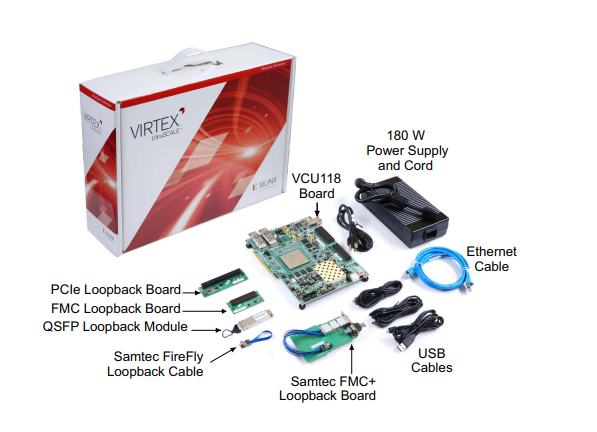
Figure1-VCU118 evaluation kit
VCU118 Benefits
- RLDRAM3 (2x36-bit) memory and dual 80-bit DDR4 component memory
- PCIe Gen3 x16 with dual QSFP28 connections (VCCINT = 0.85V)
- Samtec FireFly interface, VITA 57.4 FMC+ interface, and VITA 57.1 FMC interface
- The JTAG header is available for use with AMD download cables, like the USB II platform cable.
- SGMII (10/100/1000 Mbps Ethernet), two 4x28 Gbps QSFP28 cages available
- PMBUS and system controller MSP430 for I2C bus switching, power, timers, and SD cards
- A pair of 4 GB DDR4 component memory interfaces, each with five [256 Mb x 16] devices
- Users and status LEDs display
- 12V wall adapter or ATX power
VCU118 Board KIT CONTENT
- VCU118 Evaluation Board
Featuring the Virtex UltraScale+ XCVU9P-L2FLGA2104E FPGA
- Samtec FMC+ Loopback Cards
- FMC, FMC+, and PCIe Loopback Cards
- Power Cords and Adapter
- ATX PCIe Minifit Jr Power Adapter
- Vivado™ Design Suite: Design Edition Voucher Code
Node-locked & Device-locked to the XCVU9P FPGA, with 1 year of updates
- QSFP+ Universal Loopback Adapter
- Ethernet Cable
- USB Micro Cable
- Samtec FireFly Loopback Cable
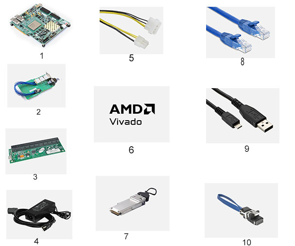
Figure2-CU118 Board KIT CONTENT
VCU118 Block Diagram
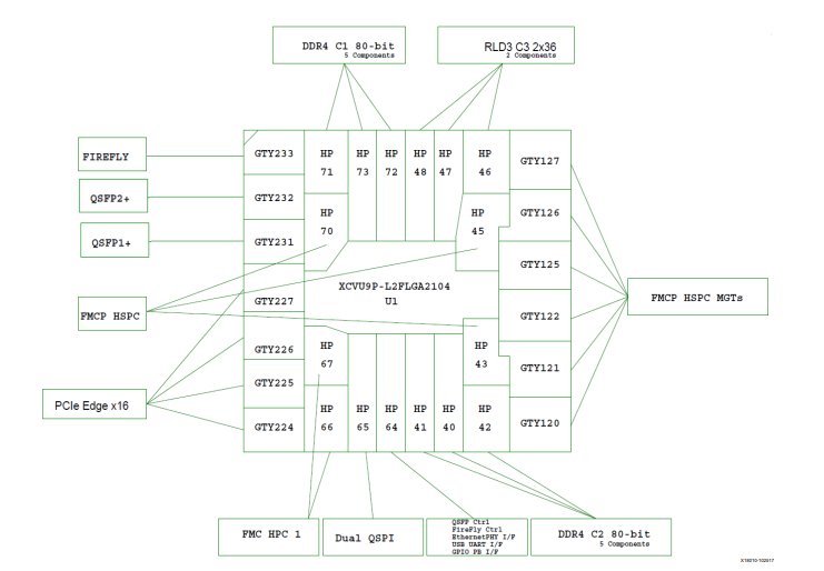
Figure3-VCU118 Block Diagram
VCU118 PRODUCT GUIDES
VCU118 LAYOUT
Featuring the Virtex™ UltraScale+™ XCVU9P-L2FLGA2104E FPGA
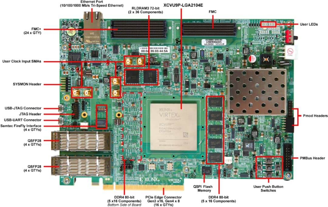
Figure4-VCU118 LAYOUT
VCU118 Board Features
Configuration
- Onboard JTAG configuration circuitry to enable configuration over USB
- JTAG header provided for use with AMD download cables such as the Platform Cable USB II
- QSPI flash memory
Communication & Networking
- 10/100/1000 Mbps Ethernet (SGMII)
- Dual 4x28 Gb/s QSFP28 cages
- Samtec FireFly 4x28 Gb/s Interface
- Dual USB-to-UART Bridge with mico-B USB connector
- RJ45 Ethernet connector
- PCI Express endpoint Gen3 x 16
Expansion Connectors
- FMC+ HSPC connector (24 – 28 Gb/s GTY Transceivers, 80 differential user-defined pairs)
- FMC HPC1 connector (58 differential user-defined pairs)
- PMOD header
- IIC
Control & I/O
- User Push Buttons (x5)
- User DIP Switch (4-position)
- PMBUS & System Controller MSP430 for power, clocks, SD-Card and I2C bus switching
Memory
- Two 2.5 GB DDR4 80-bit component memory interfaces (five [256 Mb x 16] devices each)
- 4 MB RLD3 component memory interfaces (five [256 Mb x 16] devices each)IIC EEPROM: 8Kb
- Micro Secure Digital (SD) connector 1Gb Quad SPI Flash
Clocking
- SI5335A Quad Clock Generator
- Si570 IIC Programmable LVDS Clock Generator
- SI5328C Clock Multiplier and Jitter Attenuator
- 2x SMA MGT Reference Clock inputs
- 1 SMA User Clock input
Display
- Users & Status LEDs
Power
- 12V wall adapter or ATX
VCU118 circuit diagram in the backup battery circuit
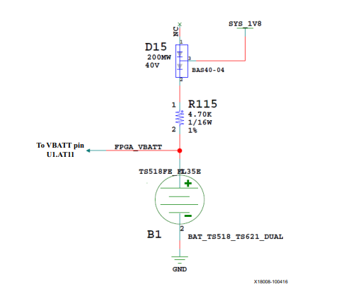
Figure5-Encryption Key Backup Circuit
With bitstream encryption key technology, the XCVU9P device U1 is utilized. The Figure 5 backup battery circuit for the encryption key is provided by the VCU118 board. With its positive output linked to the XCVU9P device U1 VBATT pin AT11, the Seiko TS518FE rechargeable 1.5V lithium button-type battery B1 is wired to the board. Under no power conditions, the maximum battery supply current (IBATT) is 150 nA. The SYS_1V8 1.8V rail charges B1 via a 4.7 K⁗ current limit resistor and a series diode with a typical forward voltage drop of 0.38V. It is 1.42V nominally when charging.
 Infineon's profit decreases, memory Q2 contract price increase revised upwards5/9/2024 11
Infineon recently announced its results for the second quarter of fiscal year 2024. Revenue was 3.632 billion euros, down 12% year-on-year and 2% month-on-month; profit was 707 million euros, down 40% year-on-year and 15% month-on-month; gross profit margin was 38.6%. , a year-on-year decrease of 8 percentage points and a month-on-month decrease of 4.6 percentage points.
Read More > NXP and ON Semiconductor released financial reports5/5/2024 26
NXP and ON Semiconductor released financial reports, rising copper prices were transmitted to the IC industry
Read More > Tesla cuts 10% of global layoffs, Samsung increases NAND flash memory production this quarter4/17/2024 28
1.Tesla announced 10% of its global layoffs, with a higher domestic proportion
Read More > How much do you know about fpga design engineer?4/16/2024 54
Circuitry can be a complex field. The circuit must be completely redone because even the smallest error can drastically alter the project's outcome. One of the numerous individuals involved in circuit building is the FPGA design engineer.An electrical engineer with a focus on designing Field Programmable Gate Array integrated circuits is known as an FPGA engineer.After reading this site, you will be fully informed about fpga design engineers.
Read More > Renesas starts up old factory to increase power device production4/15/2024 32
Renesas Electronics announced in December that the Kofu factory that had previously ceased operations was reactivated. As a 300mm wafer fab, the plant will begin mass production of IGBTs and other products in 2025, doubling Renesas' current power semiconductor production capacity. Renesas held an opening ceremony on April 11, which was attended by local government officials and partner companies.
Read More >
Hot News
- Diode Overview: Application in Automotive Alternator Rectifiers
- Ultra-low power consumption of STM32U575/585 microcontrollers(MCU)
- The Best Guide to Transistor
- Basic Information about Temperature Sensor
- Electronic Component Symbols: Resistor, Capacitor, Transformers and Connectors
- Voltage-Controlled Oscillator: Principle, Type Selection, and Application
SUPPORT
ABOUT BITFOIC
QUICK LINKS
Connect with us
Tel: 86-755-23606554
E-mail: [email protected]
Address: Room A29, 24 / F, Hoi Tak Wai, Prince Edward industrial building, 706 Prince Edward Road East, San Po Kong, Kowloon,Hongkong
Mon-Fri: 09.30 AM - 18.30 PM


