


A Comprehensive Guide to Xilinx Zynq 7000
Introduction
Xilinx ZYNQ 7000 is a fully programmable System-on-Chip (SOC), comprised of a combination of FPGA and ARM components. With hardware and software programmability, it exhibits distinct advantages across various application scenarios. This article, based on information from the official Xilinx website and incorporating data from multiple ZYNQ-7000 datasheets, consolidates essential details about the product. This topic covered Xilinx ZYNQ 7000 basics including resource overview, speed grades, temperature grades, nomenclature conventions, and architectural insights, aiming to facilitate a comprehensive understanding of ZYNQ.
Table of Content
1. What is SOC?
SOC: System On Chip, also known as Programmable SOC, is called a fully programmable system on a chip.
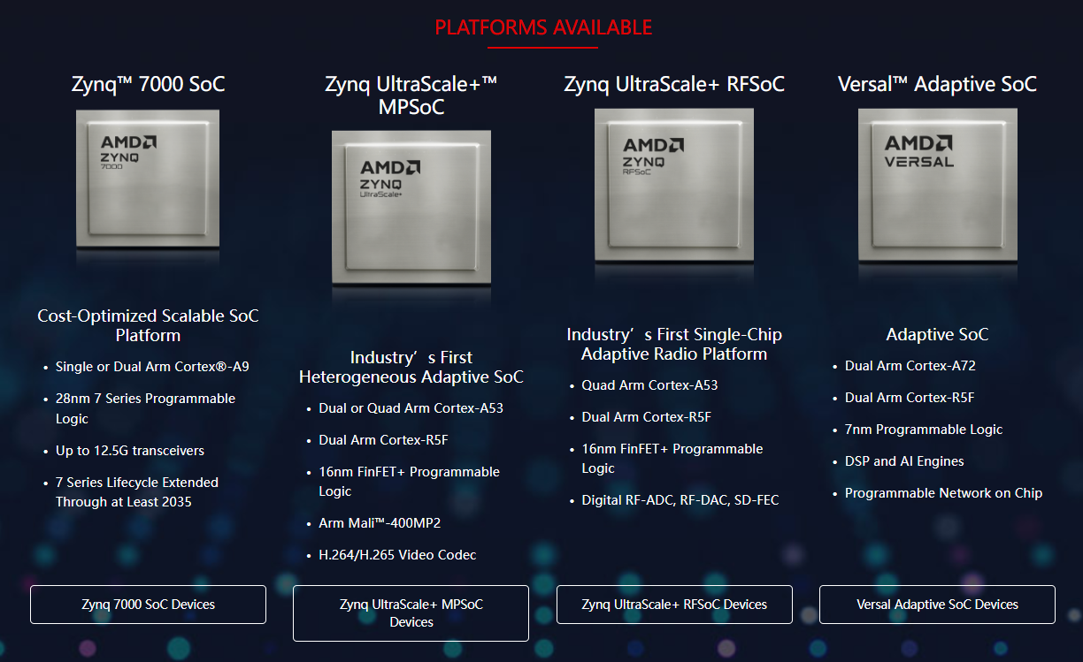
Figure1-soc
4 series Xilinx SOC
ZYNQ 7000, this series is the first-generation SOC architecture chip released by Xilinx in 2015. It is also the world’s first SOC chip series.
ZYNQ UltraScale+ MPSoC, powerful performance
ZYNQ UltraScale+ RDSoC, powerful performance
Versal ACAP, the latest chip released by Xilinx, also has the strongest performance
The SoC (System-on-Chip) integrates one or multiple ARM processor cores with one FPGA, combining software-programmable hard-core processors and hardware-programmable FPGA on a single chip. The ability to program software and hardware is why the SoC is referred to as a fully programmable System-on-Chip.
The ARM processor in the SOC is called PS (Processing System), while the FPGA is called PL (Programmable Logic). SOC = PS + PL, among which PS is the main one. Like a separate ARM chip (such as ST's STM32 series), PS is equipped with multiple peripherals, such as a serial port, CAN port, GPIO, etc. The PL part can be regarded as A "programmable peripheral" for PS.
Some people may have doubts: since SOC = PS + PL, then using a combination of an ARM chip and an FPGA, regardless of area cost and other issues, will the performance be the same as SOC? Certainly not. In the same chip, PS and PL in ZYNQ can perform low-latency and high-speed intra-chip communication, but it is tough to achieve low-latency and high-speed inter-chip communication between the two chips. This is one of the main advantages of SOC.
- Advantages of SOC: 1. Flexible, 2. Low cost
- Disadvantages of SOC: 1. Development is difficult, developers should be familiar with both FPGA and ARM
Reference: https://www.xilinx.com/products/silicon-devices/soc.html
2. Xilinx ZYNQ 7000 series product
Xilinx ZYNQ 7000 SOC is divided into two types of products: ZYNQ-7000S and ZYNQ-7000. The S in 7000S is the abbreviation of Single, which means that the 7000S chip only integrates one A9 core, while the 7000 has two.
Processing System (PS)
|
Features |
Zynq 7000S |
Zynq 7000 |
|
|
Devices |
Z-7007S, Z-7012S, Z-7014S |
Z-7010, Z-7015, Z-7020 |
Z-7030, Z-7035, Z-7045, Z-7100 |
|
Processor Core |
Single-core ARM® Cortex®-A9 MPCore™ |
Dual-core ARM Cortex-A9 MPCore |
|
|
Maximum Frequency |
Up to 766MHz |
Up to 866 MHz |
Up to 1GHz |
|
External Memory Support |
DDR3, DDR3L, DDR2, LPDDR2 |
||
|
Key Peripherals |
USB 2.0, Gigabit Ethernet, SD/SDIO |
||
|
Dedicated Peripheral Pins |
Up to 128 |
Up to 128 |
128 |
Reference: https://www.xilinx.com/products/silicon-devices/soc/zynq-7000.html
2.2 Resource Overview
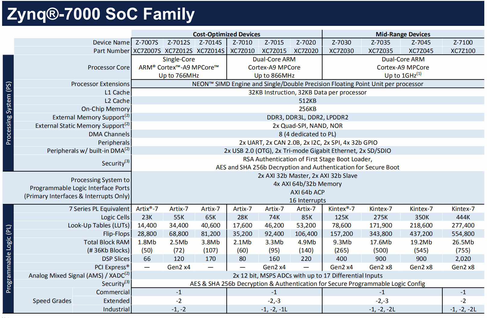
Figure2-Resource Overview
The main differences between 7000 series chips are:
- Number of processor cores
- Processor frequency
- PL resources, but there is no difference in peripherals.
2.3 Speed and temperature
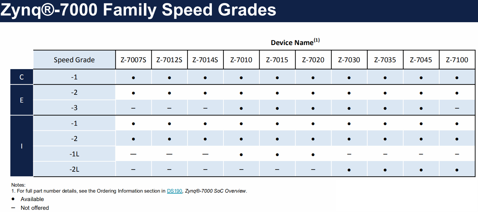
Figure3-Speed and temperature
There are 3 speed levels, -1 is the slowest, -2 is medium, and -3 is the fastest. With L means Low Power (low power consumption)
There are three temperature levels:
C, Commercial, commercial grade, 0~85℃
E, Extended, extended level, 0~100℃
I, Industrial, industrial grade, -40~+100℃
2.4 Chip naming rules
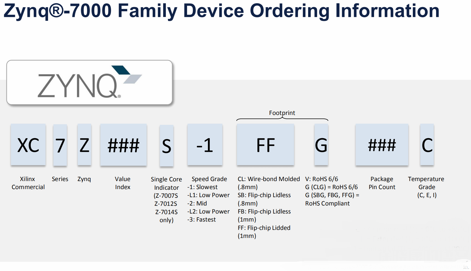
Figure4-Chip naming rules
For example, XC7Z020-2CLG484I means that the chip is ZYNQ-7020, speed level -2, and an industrial-grade chip encapsulating CLG484.
3. Xilinx ZYNQ 7000 Datasheet
3.1 Xilinx ZYNQ 7000 Description
The Zynq-7000 series is based on Xilinx's first-generation SoC architecture. These products integrate a feature-rich dual- or single-core ARM Cortex-A9-based processing system (PS) and 28nm Xilinx programmable logic (PL) in a single device. ARM Cortex-A9 CPU is the core of PS, including on-chip memory, external memory interfaces, and rich peripheral interfaces.
The Zynq-7000 series provides the flexibility and scalability of FPGAs while providing the same performance and power as commonly used ASICs (Application Specific Integrated Circuits) and ASSPs (Application Specific Standard Parts) and ease of use. At the same time, the Zynq-7000 series provides industry-standard design tools (Vivado, SDK, Vitis, etc.), allowing designers to develop cost-sensitive and high-performance applications using a single platform. Each device in the Zynq-7000 series contains the same PS, but PL and IO resources vary between devices. Therefore, Zynq-7000 and Zynq-7000S SoC can meet a variety of application scenarios.
Zynq-7000 integrates PS and PL, implements custom logic in PL, and implements custom software in PS. The combination of the two implements multiple functions. Two-chip solutions (FPGA + ASSP) cannot achieve the same performance level due to I/O bandwidth, latency, and power consumption.
Xilinx provides a large amount of soft IP for the Zynq-7000 series. ARM-based PS also integrates with Xilinx’s existing PL ecosystem, bringing a wide range of third-party tools and IP providers.
PS and PL can work independently or run operating systems, such as Linux, on PS. Xilinx also offers other standard operating systems.
PS and PL are located on separate power domains, and the PL power can be turned off when the PL is not in use. The processor in the PS always starts first, allowing a software-centric approach to PL configuration. Configuration of the PL is managed by software running on the CPU, so the startup of ZYNQ is similar to ASSP.
3.2 Xilinx ZYNQ 7000 Architecture Overview
As shown in the figure above, PS contains four major blocks:
- Application processor unit (APU),
- Memory interfaces,
- I/O peripherals (IOP),
- Interconnect,
Note: The PS architecture of ZYNQ-7000 series chips is the same.
4. Explore PS architecture
4.1 APU
APU Including:
- Single/two A9 cores, the 7000S APU has only a single core, missing the dotted box in the upper right corner of the picture above
- SWDT(System Watch Dog Timer,
- TTC(Triple Timer/Counter,
- System-Level Control Regs
- DMA 8 Channel(Direct Memory Access,)
- GIC( General interrupt controller,)
- Snoop Controller,AWDT(ARM Watch Dog Timer),Timer
- 512KB L2 Cache & Controller
- OCM Interconnect 256K SRAM
Each A9 core includes:
- FPU and NEON Engine(Float Point Unit)
- MMU(Memory Management Unit)
- A9 CPU(central processing unit)
- 32KB I-Cache(Instruction Cache)
- 32KB D-Cache(Date Cache)
4.2 Memory interfaces
As you can see from the picture above, there are two memory interfaces, the lower left side, and the middle right side.
Three interfaces on the left:
- SRAM/NOR,
- ONFI 1.0 NAND
- Q-SPI CTRL
These three types are connected to non-volatile memories such as FLASH.
The DDR interface for volatile memory on the right side supports DDR2/3, DDR3L, LPDDR2,
4.3 IOP (Input/Output Peripheral)
Input/output peripherals, input/output peripherals, are located on the left side of the picture above. The peripherals from top to bottom are:
2-way USB
2-way GigE (Gigabit Ethernet, Gigabit Ethernet)
2-way SD SDIO (SD card interface SDIO, Secure Digital Input and Output, secure digital input and output)
GPIO (General Purpose Input Output, general purpose input and output)
2-way UART (Universal Asynchronous Receiver/Transmitter, Universal Asynchronous Receiver/Transmitter, referred to as serial port)
2-way CAN (Controller Area Network, controller area network)
2-way I2C (Inter-Integrated Circuit Bus, Bus is omitted, called integrated circuit bus)
2-way SPI (Serial Peripheral Interface, serial peripheral interface)
4.4 Interconnect
Connect processors, memory interfaces, peripherals, etc.
5. Interface between PS and PL
The communication between PS and PL is carried out through some interfaces, as follows:
- AXI interface, high-speed communication port between PS and PL
- DMA interrupt
- EMIO
- Clock and reset, PS can provide clock and reset signals to PL
- Processor configuration access port (PCAP), processor configuration port, PS can configure PL through this port
- XADC interface, ADC on Xilinx chip
- JTAG, programming, and online debugging
 A Comprehensive Guide to Grasping FPGA Structure6/20/2024 697
FPGA (Field-Programmable Gate Array) is an integrated circuit, a type of programmable chip, that allows engineers to program custom digital logic. It can change its hardware logic based on the program, with the primary purpose of enabling engineers to redesign and reconfigure their chips faster and cheaper, whenever they want. However, nothing in the world is ideal, and FPGA chips also have limitations!
Read More > The EU to Impose Tariffs on Electric Vehicle Imports from China in Early July6/17/2024 349
The EU to Impose Tariffs on Electric Vehicle Imports from China in Early July
Read More > What is XC7A100T-2FG484I?6/6/2024 510
XC7A100T-1CSG324C is an FPGA-based digital signal processing board, which consists of Xilinx's Virtex-7 series chips and FPGA interface chips.
Read More > Analog cycle inventory hits bottom, AI drives flash memory demand to continue6/4/2024 517
Analog cycle inventory hits bottom, AI drives flash memory demand to continue
Read More > Micron Plans to Build a Factory in Japan, NAND Flash Prices May Remain High5/31/2024 743
Micron Plans to Build a Factory in Japan, NAND Flash Prices May Remain High
Read More >
Hot News
- Diode Overview: Application in Automotive Alternator Rectifiers
- Electronic Component Symbols: Resistor, Capacitor, Transformers and Connectors
- Voltage-Controlled Oscillator: Principle, Type Selection, and Application
- Ultra-low power consumption of STM32U575/585 microcontrollers(MCU)
- What is Xilinx 7 Series FPGA Clock Structure- -Part two
- Basic Information about Temperature Sensor
SUPPORT
ABOUT BITFOIC
QUICK LINKS
Connect with us
Tel: 86-755-23606554
E-mail: [email protected]
Address: Room A29, 24 / F, Hoi Tak Wai, Prince Edward industrial building, 706 Prince Edward Road East, San Po Kong, Kowloon,Hongkong
Mon-Fri: 09.30 AM - 18.30 PM


