


Explore the NE555 IC: A Classic Integrated Circuit
Introduction
NE555 is a classic integrated circuit widely used in various application scenarios such as timers, pulse generators, and voltage-controlled oscillators in the electronic field. Its simple design, ease of use, and stable and reliable performance make it a favorite among electronics enthusiasts and engineers. This blog will introduce the principle, working mode, and typical applications of NE555 in detail to help readers gain a deeper understanding of this classic circuit.
Catalog
| NE555 Overview |
| NE555 Pinout |
| NE555 Features |
| NE555 internal structure |
| Working Principle and Process of NE555 |
| Main working modes of NE555 |
| Common applications of NE555 |
1. NE555 Overview
NE555 is an integrated circuit whose internal structure includes three main functional modules: comparator, RS flip-flop, voltage comparator, and output stage. The external pins provide interfaces for connection with other circuit components. The NE555 is designed to provide a simple and convenient timer solution that is widely used in analog and digital circuits.
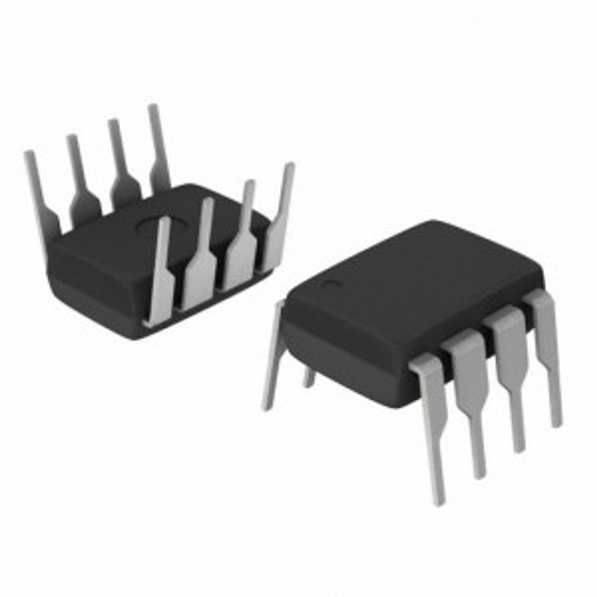
Figure1-NE555
2. NE555 Pinout

Figure2-NE555 Pinout
|
Pin |
Function |
|
Pin1(GND) |
Ground pin. It is connected to the ground (ground) of the circuit to provide the circuit's reference zero potential. |
|
Pin2(TRIG) |
trigger pin. When this pin receives a negative pulse (low-level trigger), the flip-flop will be set, causing a state change on the output pin. |
|
Pin3(OUT) |
output pin. It is used to connect the output signal of NE555. The output signal can be a square wave, pulse, etc., depending on the working mode and circuit design of NE555. |
|
Pin4(RESET) |
reset pin. When the RESET pin receives a low-level signal, it will reset the NE555 and pull the output pin low. |
|
Pin5(CTRL) |
Control voltage pin. By controlling the voltage pin, the threshold and trigger level of the NE555 can be adjusted. The CTRL pin is usually connected to the VCC pin for standard threshold and trigger levels. |
|
Pin6(THR) |
threshold pin. When this pin receives a high signal, the NE555's comparator will be reset, causing the output pin to go low. |
|
Pin7(DIS) |
Disable pin. When the DIS pin receives a low-level signal, the NE555 will be disabled and the output pin will remain in a low-level state. If disabling functionality is not required, the DIS pin can be connected |
|
Pin8(VCC) |
Positive power pin. It is connected to the positive supply to provide the supply voltage required by the circuit. |
3. NE555 Features
-
Timing From Microseconds to Hours
-
produces accurate time delays or oscillation. In the
-
Astable or Monostable Operation time-delay or mono-stable mode of operation, the
-
Adjustable Duty Cycle timed interval is controlled by a single external
-
TTL-Compatible Output Can Sink or Source resistor and capacitor network. In the a-stable mode Up to 200 mA of operation, the frequency and duty cycle can be controlled independently with two external resistors
-
On Products Compliant with MIL-PRF-38535, and a single external capacitor. All Parameters Are Tested Unless Otherwise Noted. On All Other Products, Production The threshold and trigger levels normally are twoProcessing Does Not Necessarily thirds and one-third, respectively, of VCC. These include levels that can be altered by use of the control-voltage Testing of All Parameters
4. NE555 Internal Structure
NE555 is a classic integrated circuit. Its internal circuit structure includes three main functional modules: comparator, RS flip-flop (RS Flip-Flop), voltage comparator, and output stage. The following will provide a detailed analysis of the internal circuit of NE555:
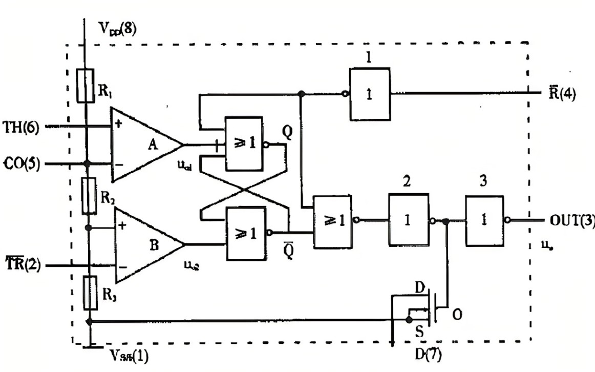
Figure3-internal circuit structure
- Comparator:
There are two comparators inside the NE555, namely the Threshold comparator and the Trigger comparator. The Threshold comparator is connected to pin 6 (THR) and the trigger comparator is connected to pin 2 (TRIG). These two comparators are used to detect changes in threshold voltage and trigger voltage.
Threshold Comparator: This comparator will output a high-level signal when the voltage rises at the Threshold pin (pin 6). When the Threshold voltage exceeds the Trigger voltage, the output of the comparator will change.
Trigger comparator: This comparator will output a low-level signal when the voltage drops at the Trigger pin (pin 2). When the Trigger voltage is lower than the Threshold voltage, the output of the comparator will change.
- RS trigger:
The NE555 contains an RS flip-flop internally to store the state of the output pin (pin 3). The input of the RS flip-flop is controlled by the outputs of the Threshold comparator and the Trigger comparator.
R input: Connected to the output of the Threshold comparator to control the reset of the RS flip-flop.
S input: Connected to the output of the Trigger comparator to control the setting of the RS flip-flop.
- Voltage comparator:
There is a voltage comparator inside the NE555 for detecting the power supply voltage. The output of this voltage comparator is connected to the RS flip-flop.
VCC detection: The voltage comparator monitors whether the power supply voltage is within the normal operating range. When the power supply voltage is too low, the comparator will output a high-level signal to reset the RS flip-flop.
- Output stage:
The output stage is connected to the RS flip-flop and controls the state of the output pin (pin 3).
The NE555 output structure is open-drain and cannot directly provide a high level. It can only pull the output pin low. Therefore, when a high-level output is required, an external pull-up resistor is usually required to remove the output pin high.
5. The Working Principle and Process of NE555
The working principle of NE555 can be divided into two stages: charging and discharging. When the power supply is powered on, the internal capacitor begins to set. When the charging voltage reaches a specific threshold, the output pin generates a high-level signal. Then the capacitor begins to discharge. When the discharge voltage reaches a specific threshold, the output pin generates a low-level signal. And so on.
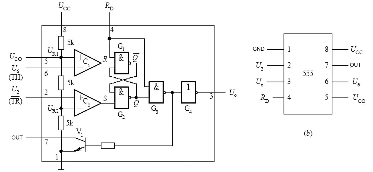
Figure4-working principle
Initial state: NE555 is in the initial state when work starts. The output pin (pin 3) is low and the RS flip-flop is in reset.
Charging Phase: When the supply voltage is applied to the NE555, the internal capacitor starts charging. The charging current passes through the resistor externally connected to the Threshold pin (pin 6), causing the voltage on the capacitor plate to gradually increase.
Threshold trigger: When the voltage of the charged capacitor reaches the comparator threshold of the Threshold pin, the Threshold comparator will output a high level. This causes the RS flip-flop to set and the output pin (pin 3) to start going high.
Discharge Phase: Once the RS flip-flop is set, a high signal at the output pin (pin 3) will cause the capacitor to discharge through the external resistor. The capacitor begins to discharge, causing the voltage at the Threshold pin (Pin 6) to decrease.
Trigger trigger: When the voltage of the discharge capacitor drops below the comparator threshold of the Trigger pin (pin 2), the Trigger comparator will output a low level. This causes the RS flip-flop to reset and the output pin (pin 3) to return to a low state.
The cycle repeats: After passing through the discharging phase, the capacitor starts charging again and the entire process repeats in a cycle. The NE555 continuously switches between the charging and discharging phases, producing a stable square wave signal.
NE555 is based on the charging and discharging process of the capacitor to control the triggering and reset behavior. By adjusting the values of external resistors and capacitors, the frequency and duty cycle of the NE555 output square wave can be changed.
6. Main working modes of NE555
NE555 has three common operating modes: monostable, multistable, and oscillator mode.
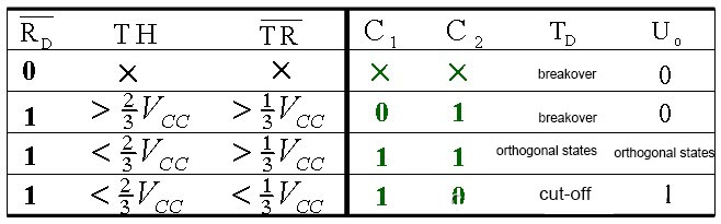
Figure5-internal circuit structure
- Monostable mode:
In monostable mode, the output pin remains low until the input trigger pulse arrives. Once the trigger pulse arrives, the output pin will transition, output a high-level signal for a period of time and then return to a low-level state.
- Multi-stable mode:
In multistable mode, the high and low states of the output pins can be switched by controlling the supply voltage. When the supply voltage is above a certain threshold, the output pin is high, and when the supply voltage is below another threshold, the output pin is low.
- Oscillator mode:
In oscillator mode, the NE555 can be used as a simple oscillator to generate a square wave signal. By adjusting the parameters of the external resistor and capacitor, the frequency and duty cycle of the output square wave can be controlled.
7. Common applications of NE555
Timing controller: NE555 can be used to implement various timing and delay operations, such as trigger delay, pulse width modulation, etc.
Flash controller: NE555 can be used to drive the flash circuit to achieve different flash frequencies and brightness by controlling the charging time and discharge time.
PWM controller: NE555 can be used as a PWM controller to adjust motor speed, light brightness, audio volume, etc.
Clock generator: NE555 can be used as a clock generator to generate stable clock signals for digital circuit synchronization.
Frequency measurer: NE555 can also perform frequency measurement by measuring the frequency of the output square wave.
Summarize:
As a classic integrated circuit, NE555 has the characteristics of simple design, easy use, stability, and reliability, and has developed a wide range of applications in the electronic field. From monostable mode to multistable mode to oscillator mode, NE555 can meet different needs and can be flexibly combined with other circuit components to expand its functionality.
However, it should be noted that the NE555 also has some limitations. First of all, the output current and voltage of NE555 are limited and are not suitable for directly driving high-power loads. Secondly, NE555 may produce larger errors at high frequencies. In addition, temperature changes may also have an impact on the performance of the NE555. Therefore, in applications with high accuracy and high-frequency requirements, other more specialized solutions may need to be considered.
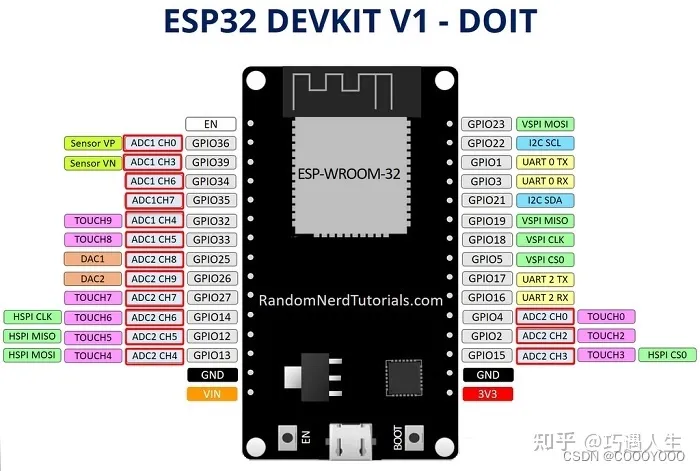 How to resolve the WiFi and ADC2 Sharing Dilemma?4/19/2024 27
ESP32-CAM can be used in various Internet of Things situations and is suitable for home smart devices, industrial wireless control, wireless Monitoring, QR wireless identification, wireless positioning system signals, and other IoT applications are ideal solutions for IoT applications.
Read More >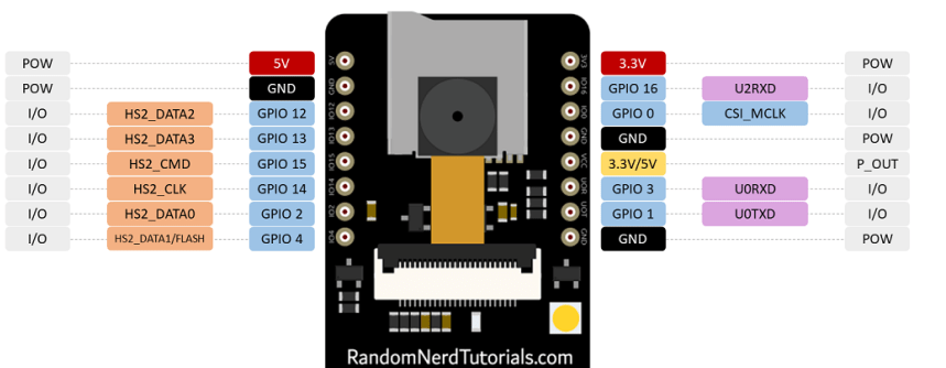 ESP32-CAM Pinout Explanation and How to Use?4/18/2024 79
ESP32-CAM is a development board with an ESP32-S chip, an OV2640 camera, a microSD card slot, and several GPIOs for connecting peripherals. ESP32-CAM is a small-sized camera module. The module can work independently as the smallest system, with a size of only 27*40.5*4.5mm.
Read More >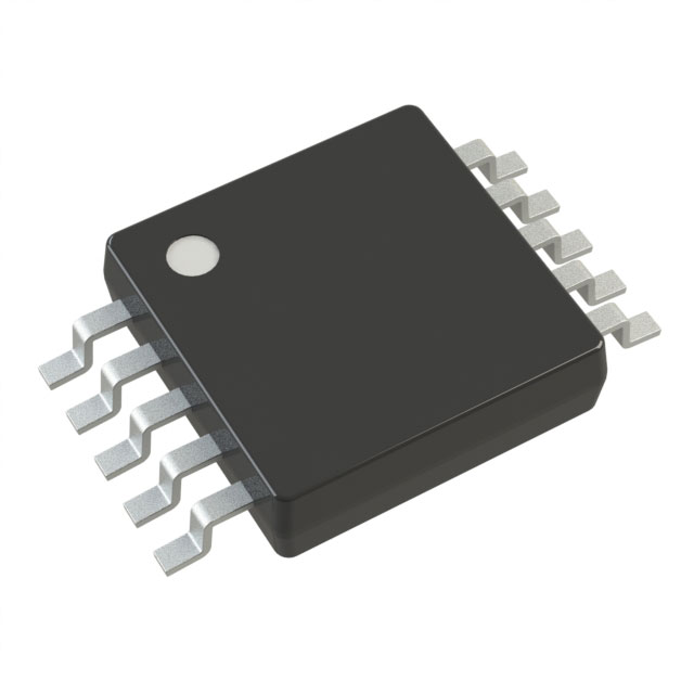 Stand-Alone Linear Li-Ion / Li-Polymer Charge Management Controller MCP738334/9/2024 63
The MCP73833/4 is a highly advanced linear charge management controller for use in space-limited, cost sensitive applications. Both a 10-lead, MSOP and a 10-lead, DFN packaging measuring 3 mm by 3 mm are offered for the MCP73833/4. In addition to its tiny size, the MCP73833/4 is perfect for portable applications because it requires a few additional components.
Read More >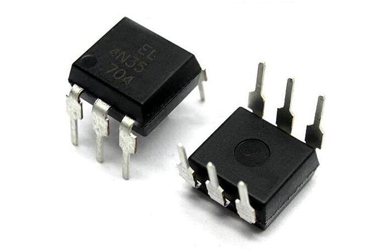 Optocoupler IC 4N35: Pinout, Datasheet, Features and Applications3/26/2024 108
In the realm of electronics, where connectivity and isolation are paramount, the 4N35 optocoupler IC stands as a beacon of reliability and versatility. This small yet mighty device plays a crucial role in ensuring signal integrity and safety across a wide range of applications. In this article, we delve into the intricacies of the 4N35 optocoupler IC, exploring its datasheet, pinout, circuit diagram, and diverse uses.
Read More > UA741CP datasheet ,Specification, Features and Application3/21/2024 111
The UA741CP is a general-purpose operational amplifier in an 8-pin DIP package. The high common-mode input voltage range and lack of latch-up make the amplifier ideal for voltage follower applications.
Read More >
SUPPORT
ABOUT BITFOIC
QUICK LINKS
Connect with us
Tel: 86-755-23606554
E-mail: contact@bitfoic.com
Address: Room A29, 24 / F, Hoi Tak Wai, Prince Edward industrial building, 706 Prince Edward Road East, San Po Kong, Kowloon,Hongkong
Mon-Fri: 09.30 AM - 18.30 PM


