


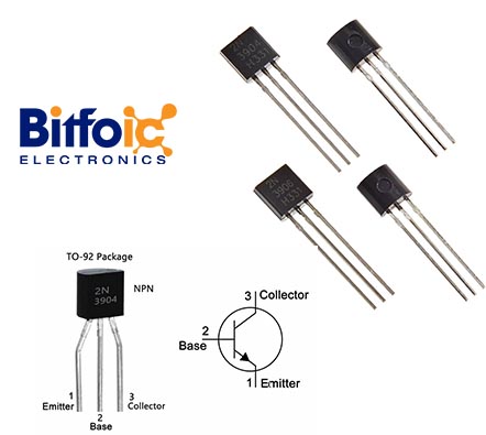
What is 2N3904 Transistor? Pinout, features and application examples
Catalog
1. What is 2N3904?
The 2N3904 is an NPN transistor used for general-purpose switching or low-power amplification applications. It is primarily designed for medium- and low-power applications and operates at moderate speed.
2N3904
2. 2N3904 pinout and pin configuration
The 2N3904 transistor consists of three pins.
- Pin 1 (Emitter): The current will flow through this terminal.
- Pin 2 (Base): This pin controls the transistor bias.
- Pin 3 (Collector): Current supply for the entire terminal.
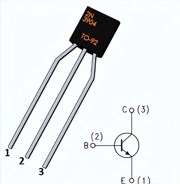
2N3904 pinout and pin configuration
|
Pin Number |
Pin Name |
Description |
|
1 |
Emitter |
Current Drains out through the emitter |
|
2 |
Base |
Controls the biasing of transistor |
|
3 |
Collector |
Current flows in through the collector |
3. 2N3904 Transistor Specification
- Collector current (Ic) (max): 200mA
- DC gain or hFE (maximum): 300
- DC gain or hFE (minimum): 100 @ 150mA, 10V
- Collector-emitter voltage (Vce): 40V
- Base to emitter voltage (Vbe): 6V
- Collector to base voltage (Vcb): 60V
- Vce saturation (maximum value) under Ib, Ic conditions: 500mV @ 50mA, 500mA
- Power – Max: 800mW
- Frequency-conversion: 100MHz
- Package/casing: TO-39-3, TO-205AD
3.2 Features
- High voltage gain: 2N3904 has a high voltage gain and is suitable for use in amplifier circuits.
- Low Noise: Transistors have a low noise figure and are useful in low-level signal amplification applications.
- High current gain: 2N3904 has a high current gain, which is suitable for driving loads such as relays and lights.
- Fast switching speed: Transistors have a fast switching speed, making them ideal for switching applications.
- Low cost: 2N3904 is cheap.
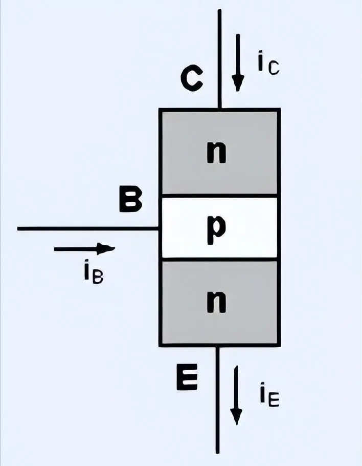
4. Working principle of 2N3904 transistor
In a 2N3904 transistor, most of the charge carriers are electrons, so they are always negatively charged. The state of this transistor can change from reverse-biased to forward-biased to conduct based on a small voltage (say 0.7V) at the base terminal.
Working principle of 2N3904 transistor
Normal working conditions:
- Base voltage (Vb) > Emitter voltage (Ve).
- Collector voltage (Vc) > Base voltage (Vb).
If the base pin is connected to the GND terminal, both the emitter and collector terminals are reverse biased or left open circuit. Likewise, once a signal is given to the base pin, it will be forward-biased.
The high gain value of the 2N3904 triode is 300, which determines its amplification capability. The maximum current supply on the collector terminal is 200mA, so loads consuming more than 200mA cannot be connected through this transistor. Once a current source is provided to the base terminal, the transistor can be biased. The IB current must be limited to 5mA.
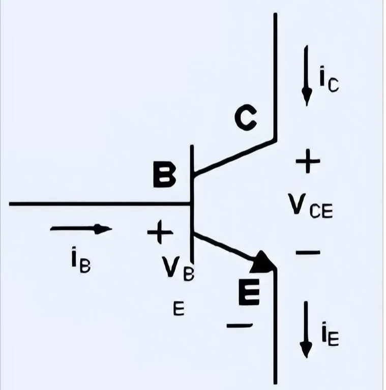
Working principle of 2N3904 transistor
When the 2N3904 NPN transistor is fully biased, it allows a maximum current of 200mA to flow through two specific terminals, the emitter and collector. This specific stage is called the saturation region. Additionally, the collector-emitter/collector-base terminals are capable of handling typical voltages of 40V and 60V respectively.
Once the base current is separated, the transistor will turn off, so this stage is called the cutoff region, and VBE may be around 600mV.
5. What transistor can be used to replace 2N3904?
1. Equivalent transistor
BC636、BC547、BC549、BC639、2N2222 TO-18、2N2222 TO-92、2N2369、2N3906、2N3055、2SC5200
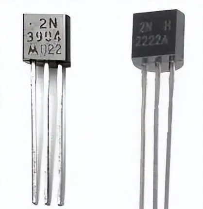
2N3904 and 2N2222
2、2N3904
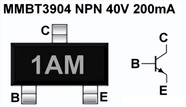
The MMBT3904 is the surface-mount version of the 2N3904, offering the same electrical characteristics but in an SOT-23 package.
You may like: MMBT3904 Transistor Basic Knowledge: Pinout, CAD Model, Package, Application and Equivalent
6. 2N3904 application examples
6.1 2N3904 as a switch
Considered a switch in electronic circuits, the 2N3904 transistor is effective, allowing larger currents or voltages to be controlled using smaller control signals. When used in switching mode, the transistor operates in the cut-off or saturation region, providing the circuit with an "on" or "off" state.
A step-by-step guide to using a 2N3904 transistor as a switch:
1) Understanding Pin Configuration
It is essential to understand the pin configuration of the 2N3904 transistor. The emitter is typically grounded (common reference), the base receives the control signal, and the collector is connected to the load or the circuit being switched.
2) Determine Load Requirements
Identify the load that the transistor switch will control. Determine the voltage and current specifications of the load, as these specifications will influence the choice of appropriate resistors and the power handling capability of the transistor.
3) Selecting the Base Resistor
Calculate the base current (IB) required to saturate the transistor and ensure it is fully "on." The base current is determined by the load current (IL) and the transistor's current gain (hfe).
To calculate the required base current:

Select a base resistor (RB) to limit the base current to a safe value, typically about 1/10th of the calculated value.
To calculate the base resistor (RB

Vcontrol is the control signal voltage.
VBE is the base-emitter voltage drop (approximately 0.7V for silicon transistors).
Connecting the Transistor
- Connect the components according to the circuit diagram:
- Connect the emitter of the transistor to the ground or a common reference point.
- Connect the collector to the positive power supply voltage and the load.
- Connect the base to the control signal through the base resistor.
- Ensure the correct polarity when connecting the load and power supply.
- Testing and Operation
Apply the control signal to the base of the transistor.
When the base current exceeds the threshold, the transistor enters saturation mode and conducts current between the collector and emitter, effectively "turning on" the load.
When the control signal is removed or reduced below the threshold, the transistor enters the cutoff region, "turning off" the load.
- Protective Measures
Use protective components such as flyback diodes or clamping circuits to suppress voltage spikes generated during switching operations, ensuring the transistor and other components functionality.
Application Example: Using the 2N3904 Transistor as a Switch
First, use the 2N3904 NPN transistor to control a simple LED on/off state as shown in the diagram below. The collector is connected to the power supply, the LED is connected to the emitter with a resistor (for current limiting), and the other end is grounded.
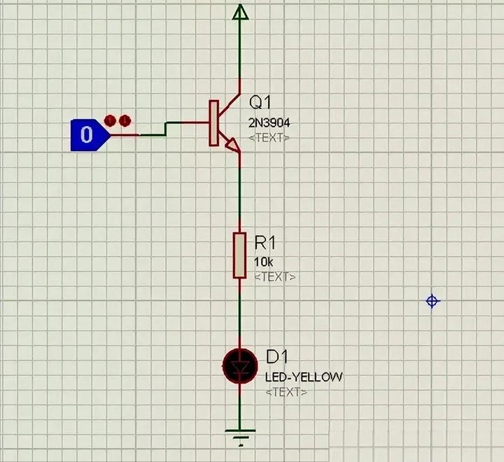
2N3904 transistor as a switch
Since no voltage is applied to the base, the 2N3904 is in a reverse-biased state, and the LED remains off. Now, when we apply a 5V voltage to the base, the 2N3904 becomes forward-biased, and the LED lights up, as shown in the diagram below:
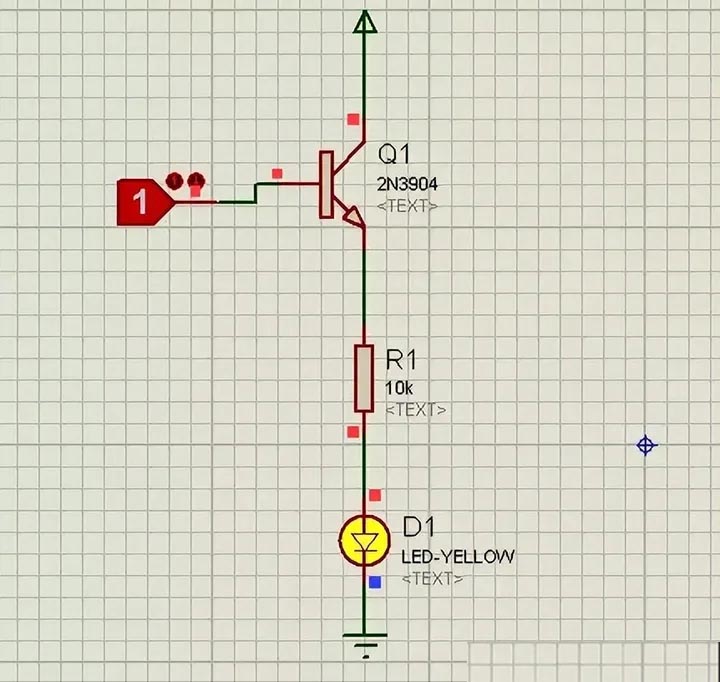
2N3904 transistor as a switch
A simple LED is controlled in the simulation above, and a manual switch is used.
6.2 2N3904 as amplifier
The 2N3904 transistor is commonly used as a general-purpose amplifier in electronic circuits. Its versatile features and usability make it suitable for a variety of applications requiring signal amplification. When used as an amplifier, the 2N3904 operates in its active region where small input signals are amplified to produce a larger output signal.
A step-by-step guide to using a 2N3904 transistor as an amplifier:
1) Pin Configuration
Familiarize yourself with the pin configuration of the 2N3904 transistor, which is the same as shown above.
2) Biasing the Transistor
Establish the proper DC bias for the transistor by applying the appropriate voltage to the base-emitter junction. This bias voltage determines the operating point of the transistor and ensures it remains in the active region. Use a voltage divider network composed of resistors to create the necessary bias voltage. For recommended biasing conditions, refer to the datasheet.
- Coupling Capacitors
Use coupling capacitors to block DC voltage, allowing only the AC components of the input and output signals to pass through. Connect one capacitor in series with the input signal at the base terminal and another capacitor in series with the output signal at the collector terminal. The capacitors prevent DC bias from affecting the input and output signals.
- Load Resistor
Connect a load resistor between the collector terminal and the positive power supply voltage. The load resistor determines the gain of the amplifier and provides a load for the amplified signal.
5) Input and Output Impedance Matching To ensure effective signal transmission between the input and output stages, match the amplifier's input impedance with the source impedance and the amplifier's output impedance with the load impedance. Impedance matching optimizes power transfer and minimizes signal reflection.
6) Testing and Adjustment Apply the input signal to the base terminal and observe the amplified output signal across the load resistor. Adjust the bias network (e.g., voltage divider resistors) to achieve the desired operating point and optimize the amplifier's performance. Use an oscilloscope or multimeter to measure and analyze the input and output signals.
7) Stability and Compensation
If necessary, add compensation components such as capacitors or resistors to improve stability and prevent the amplifier circuit from oscillating. These components are typically determined based on the amplifier's frequency response and desired bandwidth.
8) Amplifier Circuit Configurations
- Common Emitter Amplifier
- Common Collector Amplifier
- Common Base Amplifier
Among these types, the common emitter configuration is the most popular and widely used. When used as an amplifier, the transistor's DC gain can be calculated using the following formula: DC Current Gain=Collector Current (IC)Base Current (IB)DC Current Gain=Base Current (IB)Collector Current (IC)
The following is the component list:
|
|
Components |
Part number |
Quantity |
|
1 |
NPN transistor |
2N3904 |
2 |
|
2 |
NPN transistor |
2SC1815 |
1 |
|
3 |
resistor |
3.3M、820K、39K、10K、330Q |
1,1,1,1 |
|
4 |
Electrolytic capacitor |
1uF、47uF、220uF |
1,1,1 |
|
5 |
Electrolytic capacitor |
0.5w |
1 |
|
6 |
battery |
6V |
1 |
In this simple amplifier circuit using the 2N3904 transistor, any input signal needs to pass through capacitor C1. The input is fed to the base of Q1 after filtering out all signals except the audio signal. Q1 is configured as a common emitter amplifier circuit.
The voltage divider circuit for Q1 requires the connection of R1 and R2. The output signal from the collector of Q1 is insufficient. Therefore, the signal must be amplified again through Q2 and Q3. The circuit includes a Darlington pair with Q2 and Q3. Now, the signal has better gain and is driven through C3 to the SP1 speaker.
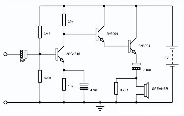
Simple amplifier circuit using transistor 2N3904
7. 2N3904 Application
- Amplifier
- Driver module (LED, motor, or relay driver)
- Switch
- Voltage regulator
- Converter
- Timer
- Frequency modulator
- PWM (Pulse Width Modulation)
- Signal processing circuit
- Audio circuit
- Power circuit
- Comparator
 DC-DC converter RFB-0505S: Specification,Datasheet,Features and Applications6/13/2024 32
The RFB-0505S is a DC-DC converter from RECOM Power, Inc., belonging to the RFB Series. It features a Single In-Line Package (SIP7) and provides a single unregulated output. This converter offers 1 watt of power with an output voltage of 5V and is rated for an isolation voltage of 1kV.
Read More > Understanding the RFMM-0505S DC-DC Converter: A Comprehensive Guide6/4/2024 98
In the world of electronics, ensuring efficient power management is crucial for the performance and reliability of devices. One of the key components in achieving this is the DC-DC converter. Today, we dive into the specifics of the RFMM-0505S DC-DC converter, exploring its features, applications, and benefits.
Read More > 12V DC-DC Converter AM2G-0512SZ: Specifications, Datasheet, Applications and Features6/3/2024 86
A DC-DC converter is an essential electronic device to convert a direct current (DC) source from one voltage level to another. These converters are widely employed in various applications, including portable electronic devices, automotive systems, and renewable energy installations.
Read More >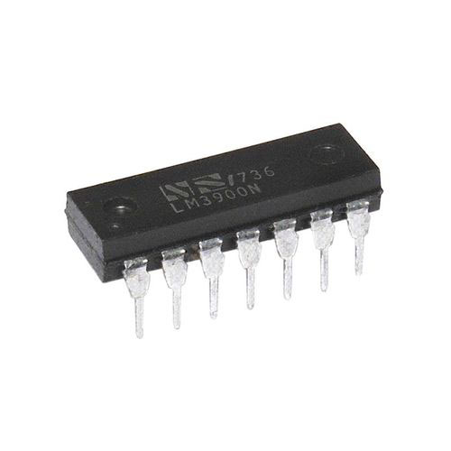 What is LM3900 Quadruple Norton Operational Amplifier?5/30/2024 118
The LM3900 consists of four independent dual-input internally compensated amplifiers. These amplifiers are specifically designed to operate on a single power supply voltage and provide a large output voltage swing. They utilize current mirrors to achieve in-phase input functionality. Applications include AC amplifiers, RC active filters, low-frequency triangle waves, square wave, and pulse waveform generation circuits, tachometers, and low-speed, high-voltage digital logic gates.
Read More > Exploring the MMBT3906 Transistor: A Comprehensive Guide5/24/2024 80
The goal of the Taiwan Semiconductor MMBT3906 PNP Bipolar Transistor is to provide a high surge current capability with minimal power loss. This transistor is perfect for automated installation and has high efficiency.
Read More >
SUPPORT
ABOUT BITFOIC
QUICK LINKS
Connect with us
Tel: 86-755-23606554
E-mail: [email protected]
Address: Room A29, 24 / F, Hoi Tak Wai, Prince Edward industrial building, 706 Prince Edward Road East, San Po Kong, Kowloon,Hongkong
Mon-Fri: 09.30 AM - 18.30 PM


