


What is Xilinx 7 Series FPGA Clock Structure- -Part two
Introduction
Welcome to the second part of our exploration into the intricate world of Xilinx 7 Series FPGA clock structures. In this installment, we delve deeper into the core elements that define the temporal heartbeat of these powerful Field-Programmable Gate Arrays.
Catalog
1. An Introduction to Xilinx 7 Series FPGA Clock Structure
The FPGA clock structure of Xilinx and the clock structure of the 7 series FPGA are very different from the clock structures of the previous series. The clock structure of the 7 series is shown in Figure 1. This picture explains the clock structure of 7 series FPGA very well. Let us have a look.

Figure1-Xilinx 7 Series FPGA Clock Structure
1 Clock Region: The FPGA is internally divided into many clock regions.
2 Horizontal Center: The FPGA is divided into upper and lower parts by the Horizontal Center, each part contains 16 BUFGs.
3 Clock Backbone: The main road of the global clock line divides the FPGA into left and right parts, and all global clock wiring must pass through this.
4 HROW: Horizontal clock line, which runs through the center area of each clock area from the horizontal direction, dividing the clock area into two parts that are completely consistent up and down. When the global clock line enters the logic resources of each clock region, it must pass through the horizontal clock line.
5 I/O Column: External signal/clock input pin.
6 CMT Backbone: For clock routing in adjacent clock regions, you can use the CMT Backbone channel included in each clock region instead of using the precious global clock network.
7 CMT Column: Each clock region contains a CMT, and a CMT consists of an MMCM and a PLL.
8 GT Column: Contains high-speed serial transceiver.
2. Internal Structure of the Clock Region
In the previous paragraph, we introduced the overall clock architecture of the 7 series FPGA. We know that the FPGA is composed of many clock regions, and the clock regions can work uniformly through the Clock Backbone and CMT Backbone. Next, we will introduce the internal structure of the clock area. The dotted box shown in Figure 2 is a clock area:
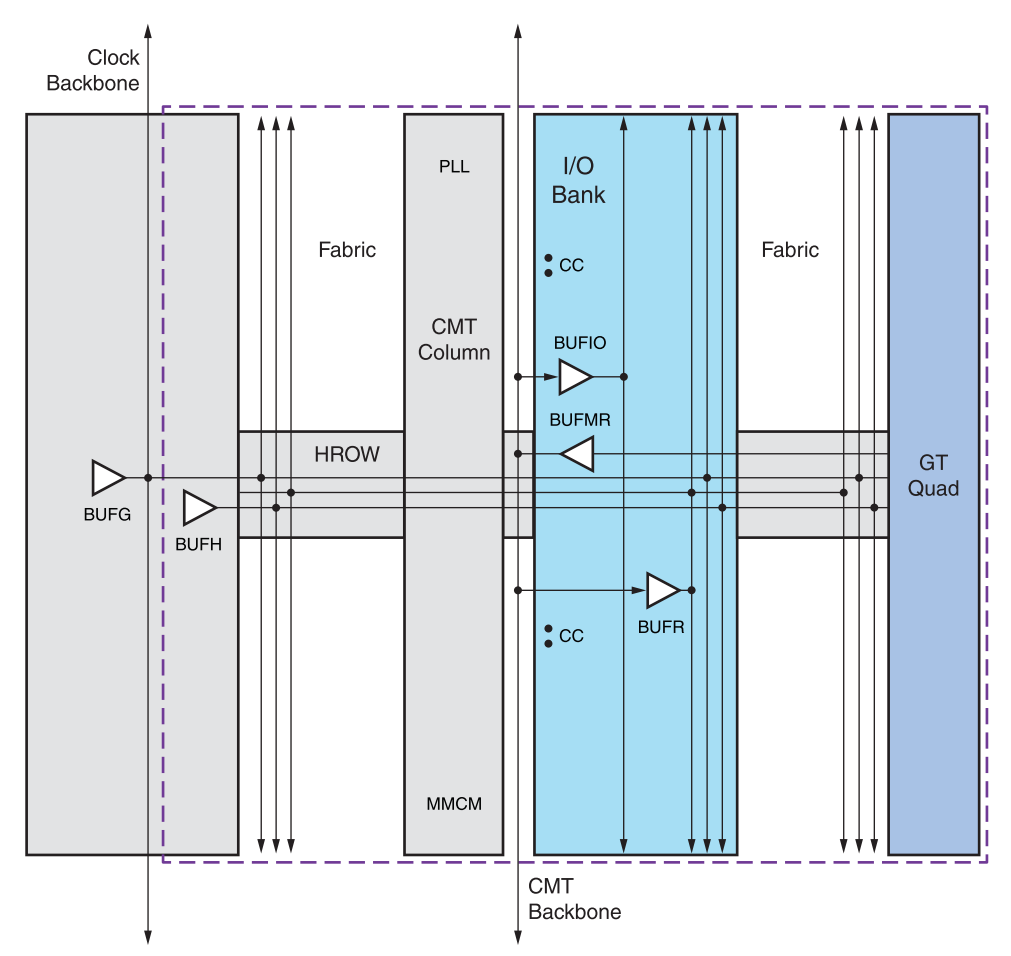
Figure2-Internal structure of the clock region
1. BUFG is the global clock buffer. As you can see from the figure, its output clock can reach any clock region through the Clock Backbone, and the BUFG reaches each logical unit inside the clock region through HROW.
2. BUFH is the horizontal clock buffer, which is equivalent to a BUFG with limited functions. Its output clock can only work in the left and right adjacent clock areas through HROW.
3. BUFIO is the IO clock buffer. Its output clock can only act on the IO register of one clock area and cannot be used in the internal logic of the FPGA.
4. BUFR is a regional clock buffer, and its output can only act on one clock region, which is equivalent to a castrated version of BUFH.
5. BUFMR is a multi-region clock buffer, and its output can be applied to the upper and lower adjacent clock regions except for this clock region through the CMT Backbone.
6. MMCM and PLL are clock management modules, which are used to eliminate clock delay and jitter and generate clocks of various frequencies.
7. CC is the external clock input pin. Its pin can be connected internally to BUFG, BUFR, BUFIO, BUFH, MMCM, PLL, etc. The user can design it independently depending on the specific application.
Generally speaking, if you are a beginner, you can know this superficially. But once it comes to the design of high-speed data transmission and reception logic in the interface, users must have a clear understanding of these clock structures before they can have a flood of ideas and write actually usable FPGA code!
3. How to Operate a Clock?
1. MRCC: driven by an external differential/single-ended clock; can drive 4 BUFIOs, 4 BUFRs, 2 BUFMRs in this clock area, CMTs in this clock area, and CMTs, 16 BUFGs, and this clock in the upper and lower adjacent clock areas region as well as the BUFH of horizontally adjacent clock regions.
2. SRCC: similar to MRCC, but only works in this clock area; it is driven by an external differential/single-ended clock; it can drive 4 BUFIOs, 4 BUFRs in this clock area, CMT in this clock area, and upper and lower adjacent clock areas CMT, 16 BUFGs, this clock region and the BUFH of horizontally adjacent clock regions.
3. BUFIO: In the same clock area, it can be driven by CLKOUT0~3 and CLKFBOUT of MRCC, SRCC, and MMCM, and can also be driven by BUFMR in this clock area and the upper and lower adjacent areas; it can only drive the BUFIO in this clock area. ILOGIC, OLOGIC.
4. BUFR: In the same clock area, it can be driven by CLKOUT0~3 and CLKFBOUT of MRCC, SRCC, and MMCM, and can also be driven by BUFMR in this clock area and the upper and lower adjacent areas; it can drive CMT, All logic units and 16 BUFGs in this clock area (not recommended).
5. BUFMR: It can only be driven by the MRCC of this clock area and some GT clocks; it can drive the BUFIO and BUFR of this clock area and the upper and lower adjacent areas.
6. BUFG: It can be driven by SRCC, MRCC, CMT, GT, BUFR (not recommended), and other BUFG in each clock region; it can drive CMT, GT clock, other BUFG, any logic unit in the FPGA, and BUFH.
7. BUFH: It can be driven by the SRCC, MRCC, CMT, BUFG, and GT clocks in this clock area and the left and right adjacent clock areas; it can drive the CMT and GT clocks in this clock area, and all logic units in this clock area. .
8. GT clock RXUSERCLK, TXUSERCLK: It can be driven by any BUFG and BUFH in this clock area; it can only drive dedicated serial transceiver modules.
9. GT clock RXOUTCLK, TXOUTCLK: It is driven by a dedicated serial transceiver module; it can drive BUFG, CMT, BUFMR, BUFH in the same clock area and BUFH in adjacent clock areas.
10. MGTREFCLK: It is driven by an external MGT clock source; it can drive BUFG, CMT, BUFMR, BUFH in the same clock region and BUFH in adjacent clock regions.
11. CMT (PLL&MMCM): It can be used by BUFG, SRCC (this clock area and upper and lower adjacent clock areas), MRCC (this clock area and upper and lower adjacent clock areas), GT (this clock area), BUFR (this clock area or The upper and lower adjacent clock areas plus BUFMR), BUFMR, MMCM/PLL.CLKOUT0~3 driver; it can drive BUFG, BUFIO, BUFR, BUFH in the same clock area, and BUFH, MMCM/PLL in horizontally adjacent clock areas.
The clock units we need to use and their usage are fully listed above (the configuration clock is not listed, and we do not need to configure the clock). When you need to use it, you can operate the clock in the above way. Is this very convenient to use?
By the way, CMT, that is, MMCM and PLL, are very important. When using FPGA, the external input clock needs to be corrected, debounced, divided, etc. by CMT before its output clock can be used. So next, let’s talk about the most important part of the clock module, CMT!

Figure3-CMT
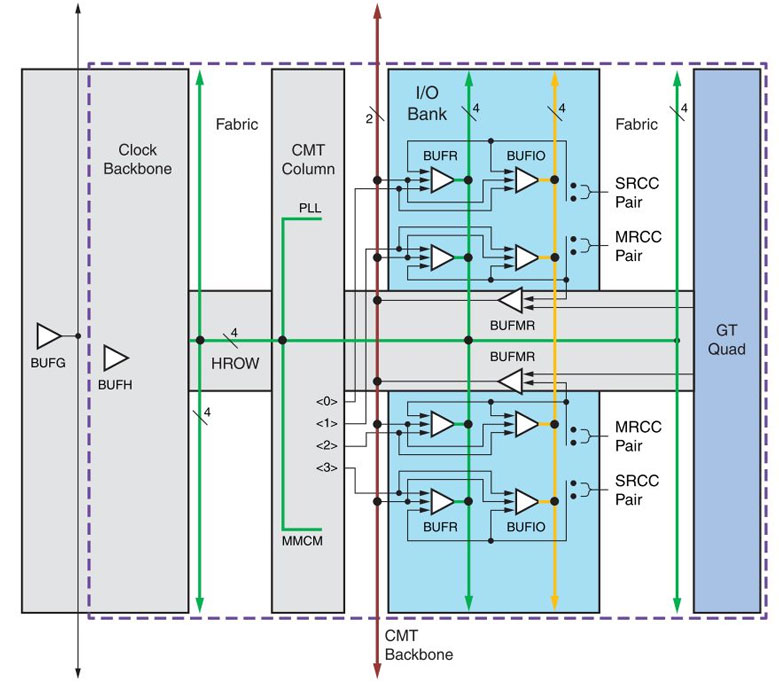
Figure4-CMT-1
The above paragraph only briefly introduces the usage of clocks without explaining them in detail, mainly because many clock usages are for specific application requirements and cannot be introduced one by one. Next, the usage of the CMT clock module will be introduced. It can be said that CMT modules should be used in every reliable FPGA design.
4. How to use the CMT Clock Module?
In the 7 series FPGA, each clock area corresponds to a CMT (clock management tile). The CMT consists of 1 MMCM (mixed-mode clockmanager) and 1 PLL (phase-locked loop). Its input is shown in Figure 5. /Output connection diagram.
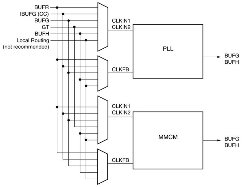
Figure 5: CMT input/output connection diagram
The functions of MMCM and PLL can be summarized in three points:
(1) Frequency synthesis: adjust the external input fixed frequency clock into multiple clocks with different frequencies
(2) Debouncing
(3) Deskew
(4) Phase operation
It is emphasized here that the PLL in the 7 series FPGA is only a functional subset of the MMCM. Here we first introduce MMCM, its structural block diagram is shown in Figure 6:

Figure6-MMCM
From the picture above, we know that MMCM has 2 clock inputs. You can choose anyone when using it. The input clock generates a certain amplitude of voltage after passing through PFD (phase-frequency detector), CP (charge pump), and LF (loop filter). Input to VCO, VCO generates a high-frequency clock with a frequency proportional to the input voltage amplitude, which is then divided by M times and fed back to the PFD. Therefore, the output frequency of the VCO is a stable high-frequency clock that is M times the input frequency. This clock can be divided by different multiples (adjustable by the user) to output clocks clkout0~clkout6. In addition, the 0th output and feedback output can be divided by fractions, and the 0th to 3rd channels provide 180-degree inverted outputs. The VCO output can also accurately adjust the phase, unique to the 7 series FPGA.
Let’s look at the structure of the PLL, as shown in Figure 7:
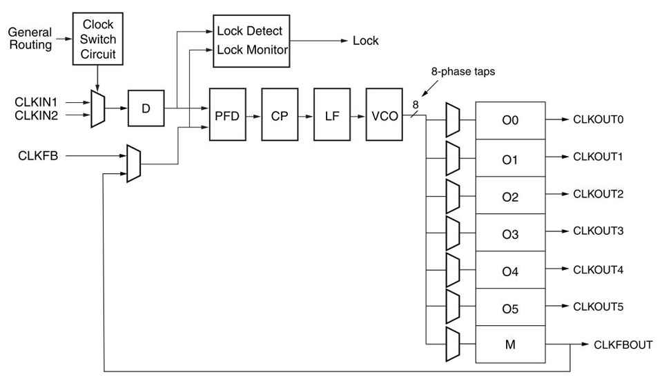
Figure 7: PLL structure block diagram
Its structure is roughly the same as that of MMCM, but it does not have the inverting output, fractional multiple division, precise dynamic phase adjustment, and CLKOUT6.
Let me emphasize here: Both MMCM and PLL can achieve frequency synthesis, debounce, and deskew at integer multiples of the clock, but MMCM can also achieve frequency synthesis at fractional times, inverted clock output, and dynamic clock phase adjustment. Of course, these high-end functions of MMCM are not used for general applications, and there is no difference between the two.
Next, we will introduce several methods of using MMCM/PLL officially recommended by Xilinx:
Figure 7 is the most commonly used usage. It is currently used the most. This design method retains the phase relationship between the input and output clocks. It has the highest clock performance and the most stable system, but it requires the use of 2 BUFGs. The BUFG is inside the FPGA. It is a scarce resource, with only 32, which may be insufficient for some particularly complex systems.
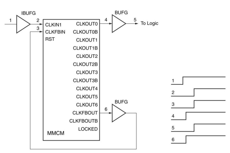
Figure 8: Phase maintaining clock design based on BUFG
Figure 8 shows BUFG replaced by BUFH. The system performance is better than BUFG. However, as mentioned in the previous paragraph, the usage range of BUFH is only the left and right adjacent clock areas. For applications that use more than 2 clock areas of logical resources, It's not appropriate.
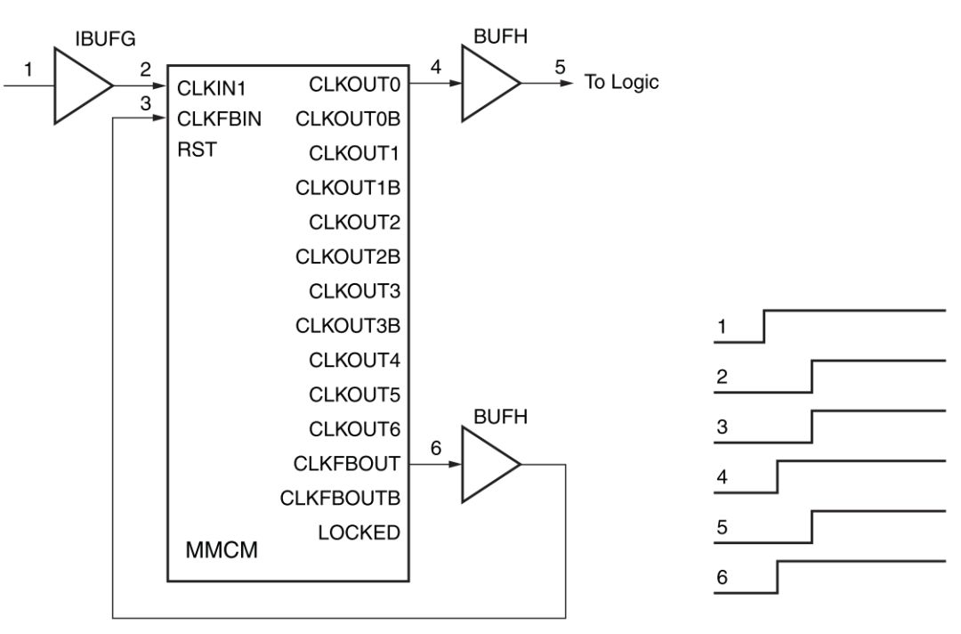
Figure 9: Phase maintaining clock design based on BUFH
Figure 10 shows the internal feedback application of the clock. Since the noise of BUFG feedback is not introduced, the noise performance of the output clock is better, but the phase relationship between the input and output clock is lost. All this usage is suitable for high-precision frequency synthesis. , applications that pay less attention to phase relationships.
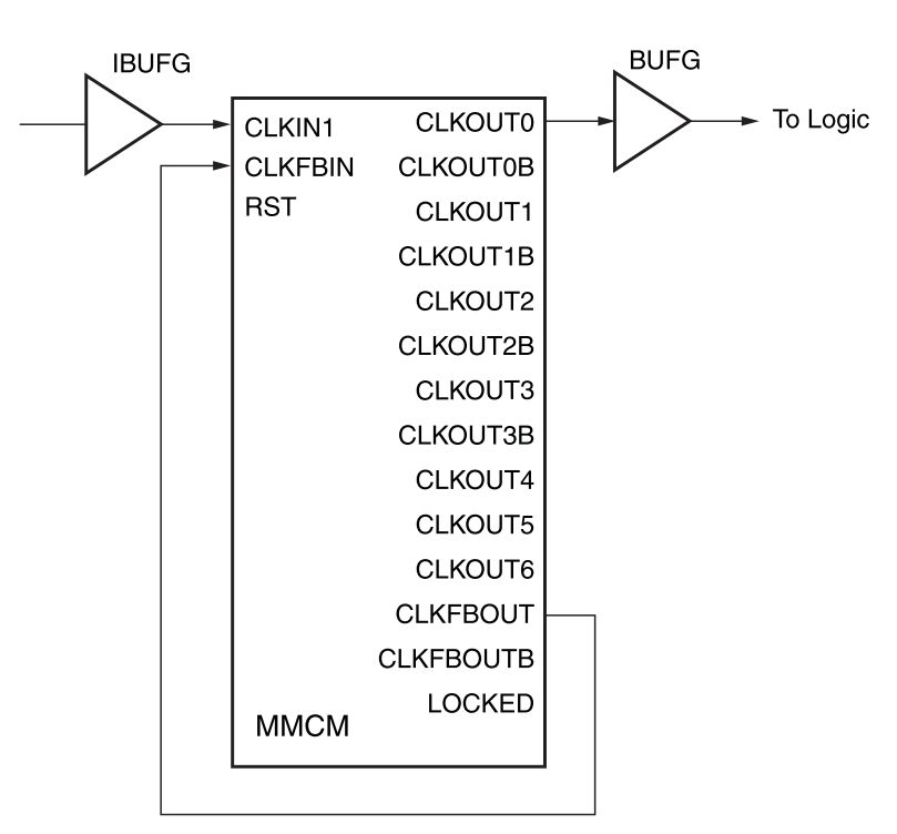
Figure 10: Low-noise clock design based on internal feedback
Figure 11 shows a zero-delay clock application, which is suitable for multiple digital systems where a single external clock source needs to maintain phase relationships.
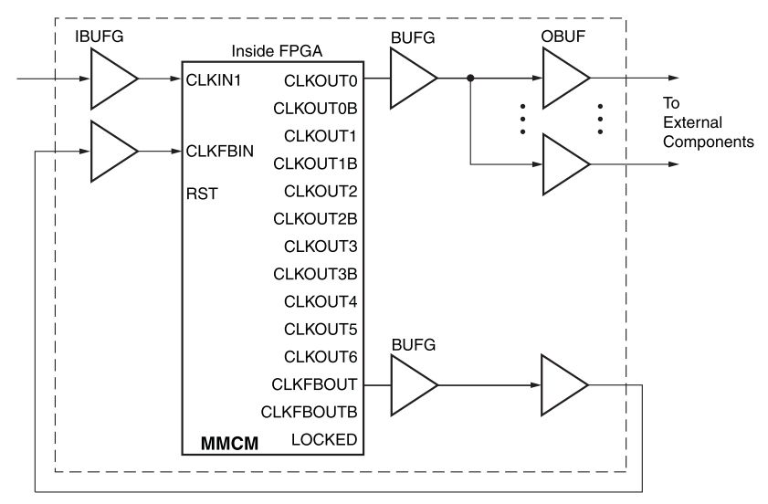
Figure 11: Multi-system clock design based on zero delay
 DC-DC converter RFB-0505S: Specification,Datasheet,Features and Applications6/13/2024 447
The RFB-0505S is a DC-DC converter from RECOM Power, Inc., belonging to the RFB Series. It features a Single In-Line Package (SIP7) and provides a single unregulated output. This converter offers 1 watt of power with an output voltage of 5V and is rated for an isolation voltage of 1kV.
Read More > Understanding the RFMM-0505S DC-DC Converter: A Comprehensive Guide6/4/2024 627
In the world of electronics, ensuring efficient power management is crucial for the performance and reliability of devices. One of the key components in achieving this is the DC-DC converter. Today, we dive into the specifics of the RFMM-0505S DC-DC converter, exploring its features, applications, and benefits.
Read More > 12V DC-DC Converter AM2G-0512SZ: Specifications, Datasheet, Applications and Features6/3/2024 537
A DC-DC converter is an essential electronic device to convert a direct current (DC) source from one voltage level to another. These converters are widely employed in various applications, including portable electronic devices, automotive systems, and renewable energy installations.
Read More > What is LM3900 Quadruple Norton Operational Amplifier?5/30/2024 1128
The LM3900 consists of four independent dual-input internally compensated amplifiers. These amplifiers are specifically designed to operate on a single power supply voltage and provide a large output voltage swing. They utilize current mirrors to achieve in-phase input functionality. Applications include AC amplifiers, RC active filters, low-frequency triangle waves, square wave, and pulse waveform generation circuits, tachometers, and low-speed, high-voltage digital logic gates.
Read More > Exploring the MMBT3906 Transistor: A Comprehensive Guide5/24/2024 776
The goal of the Taiwan Semiconductor MMBT3906 PNP Bipolar Transistor is to provide a high surge current capability with minimal power loss. This transistor is perfect for automated installation and has high efficiency.
Read More >
SUPPORT
ABOUT BITFOIC
QUICK LINKS
Connect with us
Tel: 86-755-23606554
E-mail: [email protected]
Address: Room A29, 24 / F, Hoi Tak Wai, Prince Edward industrial building, 706 Prince Edward Road East, San Po Kong, Kowloon,Hongkong
Mon-Fri: 09.30 AM - 18.30 PM


