


What is 74LS04 Hex NOT Gate IC?
Introduction
74LS04 is a member of 74XXYY IC series. The 74-series are digital logic integrated circuits.
74LS04 IC has six NOT gates. These NOT gates perform Inverting function. Hence name HEX INVERTING GATES. In this post, we will introduce 74LS04 pin configuration, Features, Application, and comparison between similar parts.
Catalog
Ⅰ 74LS04 Description
The 74LS04 is a specific type of integrated circuit (IC) that belongs to the 74LS series of TTL (Transistor-Transistor Logic) logic gates. More specifically, it is a hex inverter gate IC. The term "hex" indicates that it contains six individual inverters.
An inverter gate is a basic logic gate that takes in a digital input signal and produces the complement (inverse) of that signal at its output. In other words, if the input is high (logic 1), the output will be low (logic 0), and vice versa. The 74LS04 chip consists of six such inverters, each having a single input and a corresponding output.
The 74LS04 IC is widely used in digital electronics and is often employed in various applications, including signal inversion, waveform generation, buffering, and logic-level conversion. It operates using a 5-volt power supply and is compatible with other TTL logic families.
It's worth noting that while the 74LS04 is a commonly used IC, it's an older technology and has been largely replaced by more modern families of logic gates, such as CMOS (Complementary Metal-Oxide-Semiconductor) families like the 74HC and 74HCT series.
Ⅱ 74LS04 Pinout
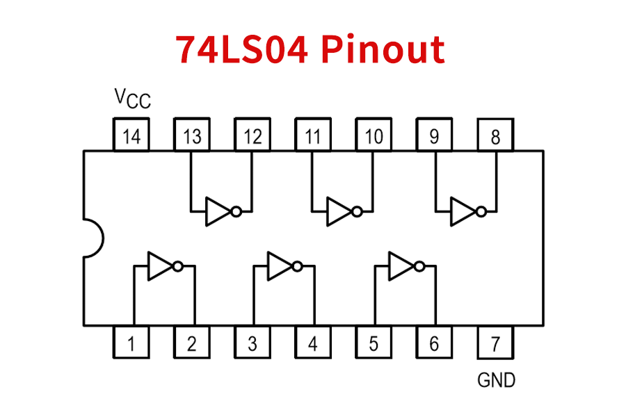
Figure1-74LS04 Pinout
74LS04 has 14 pins. The input pins of the inverting gates are pins 1, 3, 5, 9. 11, and 13. The six pins are the inputs of gates 1-6, respectively. The output pins of the inverting gates are pins 2, 4, 6, 8, 10, and 12. These are the output pins of gates 1-6. Pins 7 and 14 are shared terminals, pin 7 being the ground pin and pin 14 being the Vcc pin. The ground pin should be connected to the ground and the Vcc pin to a positive voltage.
Ⅲ 74LS04 Pin configuration
|
Pin Number |
Description |
|
INPUT OF INVERTING GATES |
|
|
1 |
1A-INPUT of GATE 1 |
|
3 |
2A-INPUT of GATE 2 |
|
5 |
3A-INPUT of GATE 3 |
|
9 |
4A-INPUT of GATE 4 |
|
11 |
5A-INPUT of GATE 5 |
|
13 |
6A-INPUT of GATE 6 |
|
SHARED TERMINALS |
|
|
7 |
GND- Should be connected to ground |
|
14 |
VCC-Should be connected to a positive voltage |
|
OUTPUT OF INVERTING GATES |
|
|
2 |
1Y-OUTPUT of GATE 1 |
|
4 |
2Y-OUTPUT of GATE 2 |
|
6 |
3Y-OUTPUT of GATE 3 |
|
8 |
4Y-OUTPUT of GATE 4 |
|
10 |
5Y-OUTPUT of GATE 5 |
|
12 |
6Y-OUTPUT of GATE 6 |
Ⅳ 74LS04 Features
- Supply voltage range: +4.75V to +5.25V
- Maximum supply voltage: +7V
- Maximum current allowed to draw through each gate output: 8mA
- Totally lead-free
- TTL outputs
- MaximumRise Time: 15ns
- Maximum Fall Time: 15ns
- Operating temperature:0°C to 70 °C
Ⅴ 74LS04 Application
- For general Logic conversion
- 74LS04 is used as an inverter in servers.
- In the memory unit, the NOT gate is used widely.
- PCs, Notebooks, and other intelligent computers come up with internal NOT gates.
- Digital electronics or any digital system like networking also use gates to invert the states.
Ⅵ 74LS04 Equivalents
CD7404, 74LS14, A single transistor can be configured to form a NOT gate.
Ⅶ 74LS04 datasheet
Ⅷ Hex NOT Gate internal
NOT gate is designed by transistors and resistors. The resistor changes the maximum current flow while the transistor serves as a switch. The power supply and resistor will be connected to the transistor. The transistor's base will function as the input and its emitter as the output. The circuit is shown here.

Figure2-NOT gate
There will be two conditions in which the circuit will operate. When input from the “A” is HIGH then the transistor will start flowing the current. The voltage from VCC will start flowing the current from VCC to Ground through the transistor and this will lower the voltages on the A’. Lowering Voltages will give the LOW state. On the other hand, when we provide the input LOW on the transistor, the transistor will not work. This will allow the power supply to give the full voltages on the output pin.
74LS04 Truth Table
The max voltages will lead the output state to HIGH in case of LOW input on the transistor. No matter how the inverter is designed. It will always give the output according to the following pattern. The input will always follow the following truth table on different inputs. All NOT gates follow the following formula A = A’.
|
INPUT |
OUTPUT |
|
0 |
1 |
|
1 |
0 |
Ⅸ Where to Use 74LS04 IC?
Here are a few cases where 74LS04 is used.
- The chip is basically used where a logic inverter is needed. Inverter Gates in this chip provide an output that is negated logic input. The chip has six gates that do NOT operate.
- When you want TTL outputs, the gates in this chip provide TTL logic outputs which are a must in some applications.
- 74LS04 is a low-cost chip available in the market and so it is used when application cost is low.
When we combine the two NOT gates in the 74LS04 integrated circuit, the output is unaffected because after the first inverter converts the state, the second inverter converts the state. When we connect any number of NOT gates in series, the output is unaffected. The effects of an even number of NOT gates will cancel one another out. Even if it is 1, 3, or 5, only the odd number permits modification. We'll use Proteus to demonstrate this condition. Connect the NOT gate to the logic state first, and then check the states to make sure they operate in accordance with the truth table above.
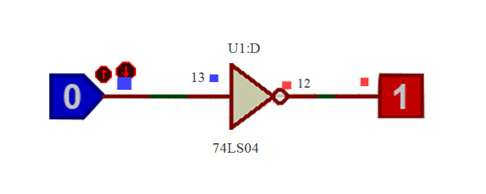
Figure3-two NOT gates
As we can see the input inverts from 74LS04 NOT gate. Now we will use two NOT gates in series and will analyze the output.
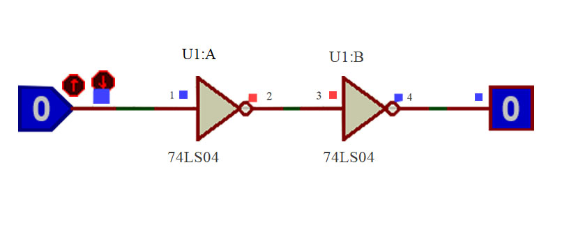
Figure4-two NOT gates in series
The odd number of gates will function in the same way as one gate. The series connection will not affect the circuit separately, but we may attach a NOT gate to the input whenever we wish to change the state of a single input in another gate. Sometimes several NOT gates are also employed to create the right circuit logic. Therefore, we must always keep in mind that several NOT gates in sequence with the same wire will impact the circuit. If multiple NOT gates attached with the same wire then we can remove them because if they are even in number then remove all of them otherwise use only one, which will minimize the circuit cost and size.
Ⅺ 74LS04 vs 74HC04
The 74LS04 and 74HC04 are both integrated circuits (ICs) that perform the same function of inverting digital signals. However, they belong to different logic families and have some key differences.
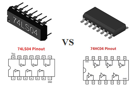
Figure5-74LS04 and 74HC04
Here's a comparison between the two:
- Logic Family:
74LS04: It belongs to the LS (Low-power Schottky) logic family. LS ICs are known for their relatively lower power consumption and slower speed than other families.
74HC04: It belongs to the HC (High-speed CMOS) logic family. HC ICs are characterized by their high-speed operation and compatibility with both TTL and CMOS logic levels.
- Voltage Levels:
74LS04 is typically designed to operate with a power supply voltage (Vcc) ranging from 4.75V to 5.25V.
74HC04 operates at a wider voltage range, usually from 2V to 6V. This makes it more versatile and compatible with a broader range of systems.
- Power Consumption:
74LS04 is known for its relatively lower power consumption than other logic families. However, it consumes more power compared to CMOS families like the 74HC04.
74HC04, the HC logic family, being CMOS-based, is known for its low power consumption. It is more power-efficient compared to the LS family.
- Speed:
74LS04 is generally slower compared to CMOS families. The propagation delay and switching times of LS ICs are higher than those of HC ICs.
74HC04 provides a faster switching speed and lower propagation delay compared to the LS family. It is suitable for applications that require high-speed operation.
- Noise Immunity:
74LS04 has good noise immunity due to its Schottky transistor technology. It can tolerate relatively higher noise levels without affecting the circuit's performance.
74HC04 also offers good noise immunity. It can handle noise levels effectively and maintain reliable operation.
When choosing between the 74LS04 and 74HC04, consider the specific requirements of your project. If you need low power consumption and can tolerate slightly slower speeds, the 74LS04 might be suitable. On the other hand, if you prioritize high-speed operation and a wider voltage range, the 74HC04 would be a better choice.
Ⅻ 2D Model
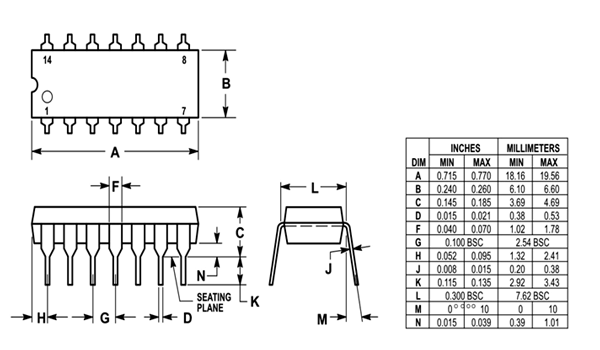
Figure6-2D Model
 DC-DC converter RFB-0505S: Specification,Datasheet,Features and Applications6/13/2024 449
The RFB-0505S is a DC-DC converter from RECOM Power, Inc., belonging to the RFB Series. It features a Single In-Line Package (SIP7) and provides a single unregulated output. This converter offers 1 watt of power with an output voltage of 5V and is rated for an isolation voltage of 1kV.
Read More > Understanding the RFMM-0505S DC-DC Converter: A Comprehensive Guide6/4/2024 630
In the world of electronics, ensuring efficient power management is crucial for the performance and reliability of devices. One of the key components in achieving this is the DC-DC converter. Today, we dive into the specifics of the RFMM-0505S DC-DC converter, exploring its features, applications, and benefits.
Read More > 12V DC-DC Converter AM2G-0512SZ: Specifications, Datasheet, Applications and Features6/3/2024 538
A DC-DC converter is an essential electronic device to convert a direct current (DC) source from one voltage level to another. These converters are widely employed in various applications, including portable electronic devices, automotive systems, and renewable energy installations.
Read More > What is LM3900 Quadruple Norton Operational Amplifier?5/30/2024 1133
The LM3900 consists of four independent dual-input internally compensated amplifiers. These amplifiers are specifically designed to operate on a single power supply voltage and provide a large output voltage swing. They utilize current mirrors to achieve in-phase input functionality. Applications include AC amplifiers, RC active filters, low-frequency triangle waves, square wave, and pulse waveform generation circuits, tachometers, and low-speed, high-voltage digital logic gates.
Read More > Exploring the MMBT3906 Transistor: A Comprehensive Guide5/24/2024 782
The goal of the Taiwan Semiconductor MMBT3906 PNP Bipolar Transistor is to provide a high surge current capability with minimal power loss. This transistor is perfect for automated installation and has high efficiency.
Read More >
SUPPORT
ABOUT BITFOIC
QUICK LINKS
Connect with us
Tel: 86-755-23606554
E-mail: [email protected]
Address: Room A29, 24 / F, Hoi Tak Wai, Prince Edward industrial building, 706 Prince Edward Road East, San Po Kong, Kowloon,Hongkong
Mon-Fri: 09.30 AM - 18.30 PM


