


Step-Down Switching Regulator LM2596: Pinout, Features, Application ans test circuits
Introduction
The LM2596 is a commonly used popular step-down switching regulator IC. The adjustable version can take in input voltage from 4.5V to 40V and convert it to variable voltage sourcing upto to 3A of continuous current. Its high current capability is commonly used in power modules to power/control heavy loads. LM2596 has been around for many years, but its sales have been thriving for a long time as its excellent performance. This post will share some details about LM2596 including its pinout, function, Features, and Applications.
Catalog
Ⅰ What is LM2596?
The LM2596 chip is divided into several types, namely LM2596, LM2596S, LM2596T, and LM2596R. These chips are only slightly different in packaging, and there is no difference in function and use. LM2596 is a non-synchronous step-down power management monolithic integrated circuit switching voltage regulator, which can output 3A drive current and has good linearity and load regulation characteristics. LM2596 internally includes a 150KHZ oscillator, 1.23v reference voltage regulator circuit, thermal shutdown circuit, current limit circuit, amplifier, comparator, and internal voltage regulator circuit, etc.
Ⅱ LM2596 Pinout
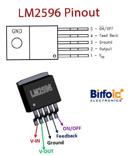
Figure1-LM2596 Pinout
1-Vin: The positive input terminal is the positive terminal of the power input of the chip. In order to prevent large transient voltages from appearing at the input terminal, an aluminum or tantalum capacitor should be added between the input terminal and the ground as a bypass capacitor. This capacitor should be close to the IC. In addition, the RMS value of the input capacitor current must be at least half of the DC load current.
2-Output: The output terminal is the output terminal of the chip, which is connected to an inductor and a diode. And the line connecting the three should be thick and short.
3-Ground: The ground terminal is part of the ground (GND). Note that in addition to the five pins of the chip, there is also a head that is also grounded (GND).
4-Feedback: The feedback terminal is the pin used by the chip itself to feed back the output voltage to ensure that the output voltage is stable and accurate.
5-ON/OFF: This pin can be used to cut off the LM2596 with a logic level, reducing the input current to about 80µA. Pulling this pin below approximately 1.3V turns the LM2596 on; pulling it up above 1.3V (up to 25V maximum) turns the LM2596 off. If you don't need to use this function, you can ground or open this pin to make the IC open.
Ⅲ LM2596 Features
- This chip is divided into four types according to functions, namely 3.3V, 5V, 12V fixed voltage output, and ADJ adjustable voltage output
- Adjustable output voltage range 1.2V~37V±4%
- Good output linearity and adjustable load
- Output current up to 3A
- Input voltage up to 40V
- Adopting an internal oscillation frequency of 150KHz, it belongs to the second-generation switching voltage regulator with low power consumption and high efficiency
- Low power standby mode, IQ typical value is 80μA
- TTL power-off capability
- With overheating protection and current limiting protection
- Package form: TO-220(T) and TO-263(S)
- The peripheral circuit is simple, only requires a minimum of 4 external components, and uses standard inductors that are easy to purchase
Ⅳ LM2596 Applications
- Used in battery circuits since they have high efficiency
- Step-down Linear regulators
- Used in small SMPS circuits
- Battery Operated Applications
- Variable Voltage generators
- Miniature RPS Circuits
Ⅴ Functional Block Diagram
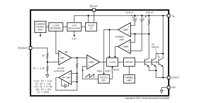
Figure2-Functional Block Diagram
Ⅵ How to use the LM2596 Regulator?
Due to its minimal component requirements, the LM2596 is relatively simple to use. The unregulated voltage is given to pin 1 (Vin) across a filter capacitor to reduce input noise. The ON/OFF or enable pin (pin 5) should be connected to ground to enable the IC. If made high the IC will enter shutdown mode and prevent leakage current. This feature will be useful to save input power when operating via battery. The crucial pin that determines output voltage is the feedback pin. It senses the output voltage and modifies the internal switch's switching frequency to produce the desired output voltage dependent on the output voltage's value. Finally, an LC filter is used to retrieve the output voltage through pin 2. The whole circuit diagram can be found in the LM2596 DC Converter module, which is provided below.
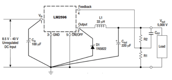
Figure3-circuit diagram
Ⅶ Test circuit and its wiring scheme
- Fixed output
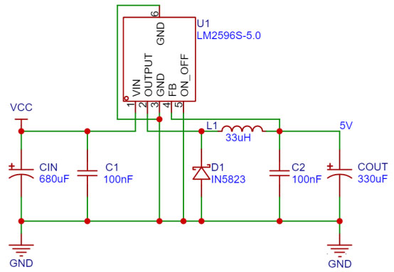
Figure4-Test circuit(Fixed output)
CIN---680μF/50V COUT---330μF/35V
D1----5A/20V IN5823 L1---33μH,L40
Note: The chip used in the picture is LM2596-5.0, even if the left input is not 12V (but higher than 5V, it is a buck chip, not a boost chip), the right side can still output a fixed 5V voltage.
- Adjustable output
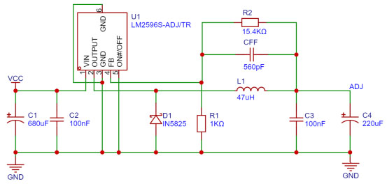
Figure5-test circuit (adjustable output )
Note: (1) The feedback line should be far away from the inductor
- The thicker and shorter lines: pin 1 and the positive pole of the capacitor, pin 2 and the cathode of the Schottky diode, pin 2 and the inductor, and the other end of the inductor and the output terminal The positive electrode of the capacitor (the negative electrode is directly covered with copper)
- The resistors R1 and R2 to adjust the output voltage should be close to the 4 pins of the LM2596.
The calculation of the output voltage can be given by:
- Vout=Vref*(1+R2/R1)
- Vref=1.23V,R2=R1*(Vout/Vref-1)
In order to ensure stable output, R1 selects a resistor with a nominal resistance of 1KΩ and an accuracy of 1%.
CIN---680μF/50V COUT---220μF/35V R1---1K,1%
D1---5A/40V IN5825 L1---47μH
CFF---Refer to relevant application information
In switching regulators, the PCB layout is crucial. The switching current is closely related to the loop inductance, and the transient voltage generated by this loop inductance often causes many issues. To minimize the inductance and ground loops, the thick lines shown in the figure should be printed wider on the PCB and kept as short as possible. The external components should be as close as possible to the switching integrated circuit (chip) to achieve the best results, and it had better use ground wire shielding or single-point grounding. It was recommended to use an inductor with a magnetically shielded construction. If the inductor used is an open core, then extra care has to be taken with its placement. The integrated circuit's ground wiring and output capacitor COUT can cause problems if the inductive flux crosses the sensitive feedback line. In an output-adjustable scheme, special attention must be paid to the location of the feedback resistor and its associated leads. Physically, on the one hand, the resistor should be close to the IC (chip), and on the other hand, the related wiring should be far away from the inductor. This is more important if the inductor used has an open magnetic core.
Ⅷ LM2596 Package
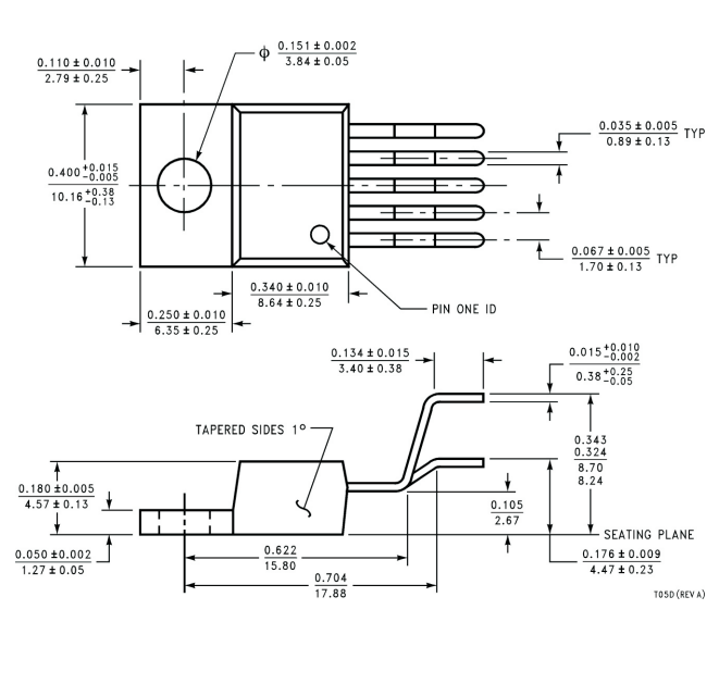
Figure6-TO-220(T) package
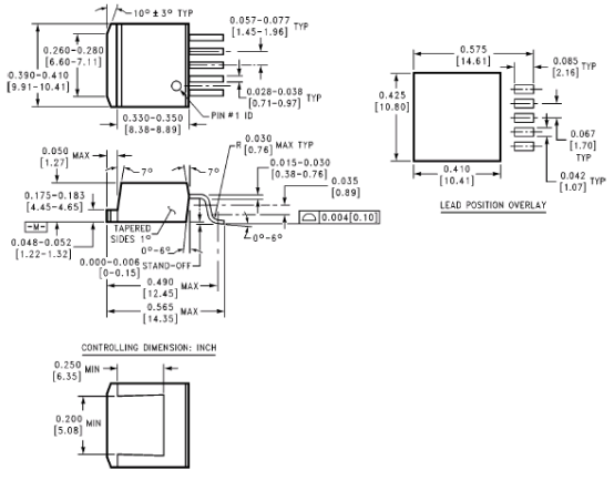
Figure7-TO-263(S)package
Ⅸ LM2596 PDF
 DC-DC converter RFB-0505S: Specification,Datasheet,Features and Applications6/13/2024 591
The RFB-0505S is a DC-DC converter from RECOM Power, Inc., belonging to the RFB Series. It features a Single In-Line Package (SIP7) and provides a single unregulated output. This converter offers 1 watt of power with an output voltage of 5V and is rated for an isolation voltage of 1kV.
Read More >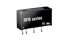 Understanding the RFMM-0505S DC-DC Converter: A Comprehensive Guide6/4/2024 768
In the world of electronics, ensuring efficient power management is crucial for the performance and reliability of devices. One of the key components in achieving this is the DC-DC converter. Today, we dive into the specifics of the RFMM-0505S DC-DC converter, exploring its features, applications, and benefits.
Read More >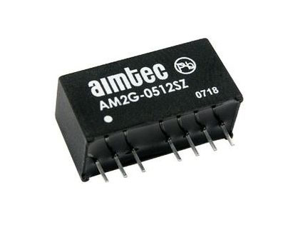 12V DC-DC Converter AM2G-0512SZ: Specifications, Datasheet, Applications and Features6/3/2024 684
A DC-DC converter is an essential electronic device to convert a direct current (DC) source from one voltage level to another. These converters are widely employed in various applications, including portable electronic devices, automotive systems, and renewable energy installations.
Read More >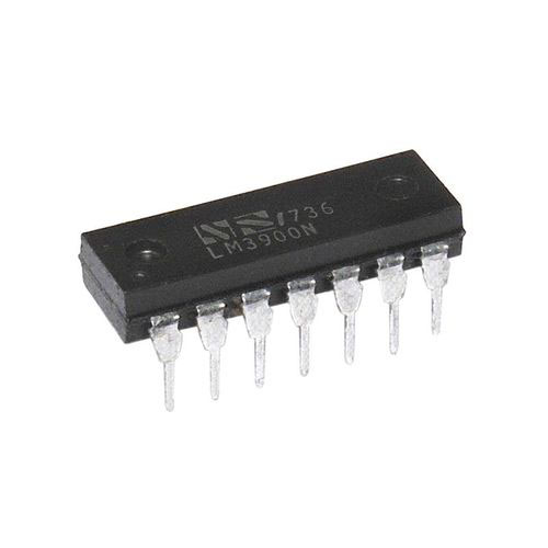 What is LM3900 Quadruple Norton Operational Amplifier?5/30/2024 1375
The LM3900 consists of four independent dual-input internally compensated amplifiers. These amplifiers are specifically designed to operate on a single power supply voltage and provide a large output voltage swing. They utilize current mirrors to achieve in-phase input functionality. Applications include AC amplifiers, RC active filters, low-frequency triangle waves, square wave, and pulse waveform generation circuits, tachometers, and low-speed, high-voltage digital logic gates.
Read More >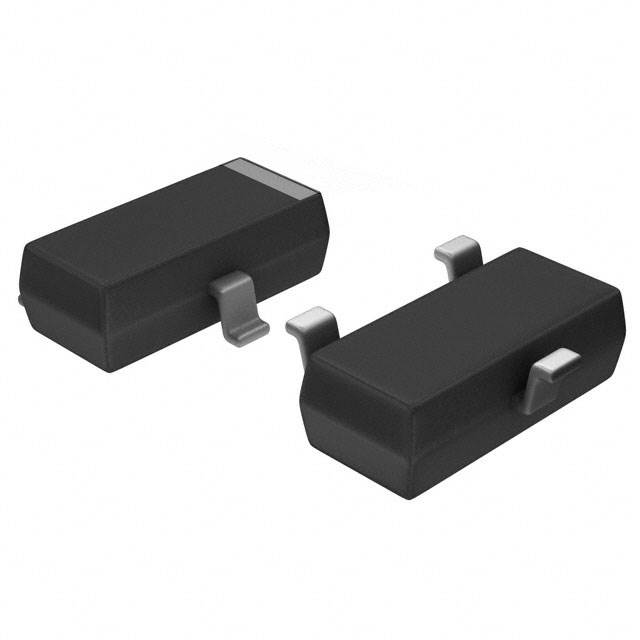 Exploring the MMBT3906 Transistor: A Comprehensive Guide5/24/2024 986
The goal of the Taiwan Semiconductor MMBT3906 PNP Bipolar Transistor is to provide a high surge current capability with minimal power loss. This transistor is perfect for automated installation and has high efficiency.
Read More >
SUPPORT
ABOUT BITFOIC
QUICK LINKS
Connect with us
Tel: 86-755-23606554
E-mail: [email protected]
Address: Room A29, 24 / F, Hoi Tak Wai, Prince Edward industrial building, 706 Prince Edward Road East, San Po Kong, Kowloon,Hongkong
Mon-Fri: 09.30 AM - 18.30 PM


