


PC817 Optocoupler IC: Pinout,Circuits,Datasheet,Features and Applications
Introduction
A type of semiconductor device known as an optocoupler, also known as an optoisolator, photo-coupler, or optical isolator, enables the transmission of electrical signals between two separated circuits by light. A photosensitive device and an LED are two parts of this component. Optoisolator integrated circuits (ICs) come in a variety of forms, including the PC817 IC, MOC3021 IC, MOC363 IC, MCT2E IC, and PC817 optocoupler.
The PC817 optocouplers are small and available in a variety of packages. It can be directly connected to any low-voltage DC device or microcontroller. The input voltage will have the same effect from each side of the optocoupler, it will just transfer the signal to the receiver, which will then have a logic signal as output. Optocouplers are versatile due to their small and compact size and their ability to be used for control operations.
Catalog
Ⅰ What is pc817?
The PC817 consists of an infrared emitting diode (IR LED) and a phototransistor optically coupled to it. An infrared emitting diode and a phototransistor are optically coupled together. Electrical signals are transmitted optically between the input side and the output side without any physical connection between the two parties.
This circuit works as long as the input signal contains some data, but when we need to transmit a signal from one element of the circuit to another, although the signal contains noise, we have to utilize a mix of IR Tx and Rx.

Figure1-pc817
In the circuit of the PC817 optocoupler, the IR takes the noise signal from one part and transmits it to the other part with the IR signal so that it performs according to the design of the circuit. The PC817 IC consists of an LED and a phototransistor optically connected. Signals can be optically transmitted between the i/p and o/p sides without any physical connection.
For any microcontroller or any DC device with a small voltage, a direct connection is possible. From every facet of the IC, the input voltage will have a similar effect; it will simply transmit the signal to the receiver. After that, the receiver will provide the logic signal as an output. This IC has many uses due to its tiny size and control operation.
Ⅱ PC817 Pinout
The diagram represents the pin configuration diagram and explains the functionality of each pin. In this pinout diagram of PC817, pin1, and pin2 are parts of the input side, and pin3 – pin4 are output pins.
The following pin configuration diagram explains the function of each pin of PC817.
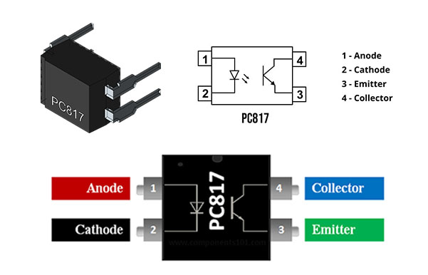
Figure2-PC817 Pinout
IR LED Input:
- Pin 1: Anode (+) pin, inputs logic signal to internal IR.
- Pin 2: Cathode (-) pin, connected to circuit and power supply common ground.
Phototransistor output:
- Pin 3: Emitter pin, establishes a common ground through the circuit and power supply.
- Pin 4: Collector pin, transmits logic output when receiving IR signal
PC817 Pin Configuration
|
Pin Number |
Pin Name |
Description |
|
1 |
Anode |
Anode pin of the IR LED. Connected to logic input |
|
2 |
Cathode |
Cathode pin of the IR LED. Connected to ground |
|
3 |
Emitter |
Emitter pin of transistor. Connected to Ground |
|
4 |
Collector |
Collector pin of the Transistor. Provides logical output |
Ⅲ How Optocoupler Pc817 Works?
The working principle of PC817 is simple, but there are specifications to use it on different devices. The optocoupler at the input needs to be current-limited with a resistor, but at the output, we need to connect the logic output pin with the power supply pin. Whenever an IR signal is generated, the logic state will change from 1 to 0 due to the change in current.
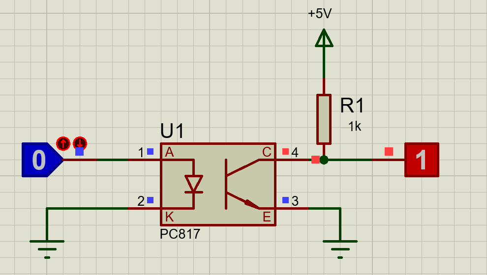
Figure3-PC817 circuit
Here connect the anode pin of the IR LED (pin 1) to a logic input which must be isolated and the cathode of the IR (pin 2) to ground, then use a resistor to pull the collector pin of the transistor high (here I Used 1K) and connected the collector pin to the output of the desired logic circuit and the emitter (pin 4) to ground.
Note: The ground of the IR LED (pin 2) and the ground of the transistor (pin 4) are not connected. This is where isolation happens.
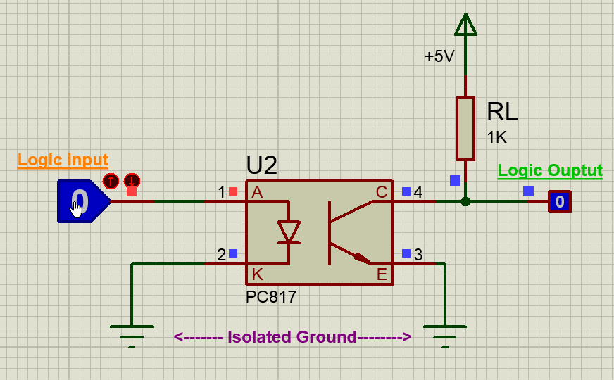
Figure4-PC817 work circuit
Now, when the logic input is low, the IR LED will not conduct, so the transistor will also be off, so the logic output will remain high. This high voltage can be set anywhere up to 30V (collector-emitter voltage), I used +5V. There is a pull-up resistor 1K acting as a load resistor.
But when the logic input goes high, this high voltage should be at least 1.25V (diode forward voltage), The IR LED turns on, so the phototransistor also turns on, which will short the collector and emitter, so the logic output voltage will become to zero. This way, the logic input will be reflected on the logic output and still provide isolation between the two.
Another important parameter to consider when using an optocoupler is rise time ( tr ) and fall time (t f ). Once the input logic goes low, the output will not go high, and vice versa. The waveform below shows the time it takes for the output to transition from one state to another. For PC817, the rise time (TPD HL ) and fall time (TPD LH ) are 18us.
1. Response time test circuit
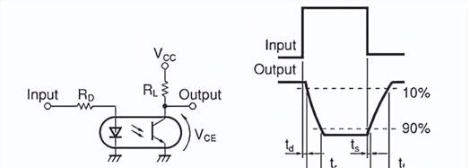
Figure5-Response time test circuit
2. Frequency response test circuit
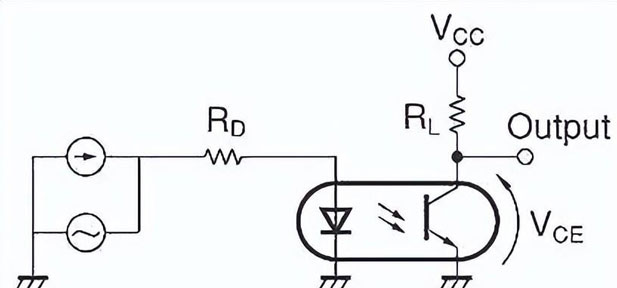
Figure6-Frequency response test circuit
Ⅳ PC817 optocoupler parameters
- High VCEO (Collector-Emitter Voltage): 80V MAX
- Input diode forward voltage: 1.25V
- Maximum collector current: 50 mA
80V maximum collector-to-emitter voltage ratio
- 4-pin DIP package and SMT package
- Internal protection of input and output
- CTR (Current Transfer Rate) available for multiple grades
Fall time: 18 μs
Rise time: 18 μs
- Cut-off frequency: 80 kHz
- Maximum power consumption: 200 mW
- High isolation voltage between input and output: 5.0kV
- The maximum operating temperature range is -30 to 100 degrees.
- The internal resistance is 100 Ω.
- The IC's internal storage temperature range is -55 to 125 degrees.
- When soldering, the temperature range of the optocoupler is 260 degrees.
Figure7-PC817 optocoupler parameters
Ⅴ PC817 Optocoupler Features
- It is available in 4-pins in both DIP and SMT packages.
- The device has an internal form of protection that is electrically isolated. Protection is for input and output. It can protect up to 5KV galvanic isolation.
- Optocouplers can be used with external resistors with high-voltage devices to work with low-voltage devices.
- Optocouplers can be used with any device that has an internal interface, such as TTL devices, microcontrollers, and even high DC voltages with some internal resistance.
- Optocoupler PC817 has internal reverse current protection.
- Due to the unidirectional current characteristics of the IR, the PC817 protects the IR from any reverse current.
Ⅵ PC817 Equivalent Replacement Model
1、PC817 Alternative Models:
4N25、6N136、MOC3021、MOC3041、6N137
2、 PC817 equivalent:
PC817A、PC817C、PC817B and PC817D
Ⅶ How to Test the Quality of PC817 Optocoupler?
1. Use a diode to detect
First, take the optocoupler, use a multimeter to measure the input end with the diode file, and replace the red and black test leads. If there is a voltage drop in the forward direction, it will be cut off in the reverse direction, indicating that the front-end LED is normal.
Connect a low voltage 6V to the input terminal (take 4N35 as an example, the specific input voltage is subject to the datasheet), connect a protective resistor in series, adjust the resistance range with a multimeter, and measure the resistance value of the other output terminal.
Disconnect the front-stage power supply with infinite power (generally megohm level), and turn on the front-stage power supply with a sharp drop in resistance value, indicating that the optocoupler works well, otherwise, it does not.
2、 Making a PC817 Optocoupler Tester Circuit
1)Test the PC817 circuit with the circuit
This circuit is primarily intended to perform a functional test of any 4-pin optocoupler IC. For functional testing, place the IC in a female header such that the emitter of the IC's phototransistor and the IR LED anode pin are connected to the circuit's GND, while the IR LED cathode and phototransistor collector pins of the IC are connected to 4V VCC.
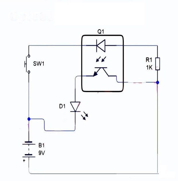
Figure8-PC817 optocoupler test circuit
Components Required
- Optocoupler IC: PC8171
- Lead: 5mm, 3.5V1
- 1 button
- 1 Resistor: 1k
- 4 female
- 1 Soldering iron: 45W - 65W
- 1 flux for soldering wire
- 1 panel
- 1 DC battery: 9V
- 1 battery clip
- Jumper: Depends on the situation
3)steps
(1) Solder two pairs of 2 female headers on the panel.
(2) Place a 1K resistor in series between the two female header pairs.
Solder the button and the female head in series.
(4) Solder the +ve terminal of the LED to the output female and the -ve terminal to the ground of the circuit.
(5) Connect the 4V DC battery to the circuit.
(6) Place the optocoupler IC in the female header, power it on, and test the circuit.
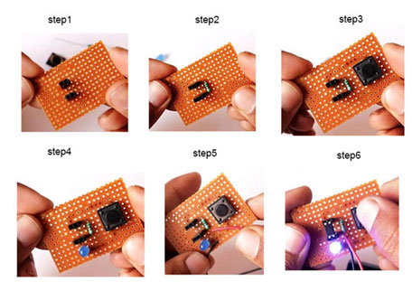
Figure: Optocoupler quality detection
Now, connect the circuit to the power supply, if the LED connected to the emitter lights up when the button is pressed, then the optocoupler IC is working fine. If the LED is off, the IC needs to be replaced.
Ⅷ PC817 optocoupler application circuit
- I/O isolation for controllers
- For general electrical isolation purposes
- Fundamental noise coupling circuits in switching circuits
- IoT devices
- Signal transmission
- Isolation of digital and analog circuits
- AC/DC power control
Ⅸ 2D-Model and Dimensions
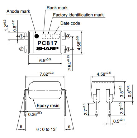
Figure10-2D-Model and Dimensions
Ⅹ PC817 PDF
This entire post is a summary of the datasheet for a PC817 optocoupler or optoisolator. Because of the expanding IoT industry, this IC provides several advantages. As a result, it is frequently used in daily life to manage various equipment. This IC aids in the design of electronic circuits where voltage spikes or surges could potentially harm the circuit's components.
As a result, this IC aids in circuit isolation. Additionally, it is employed to separate AC and high-voltage circuits from DC and low-voltage circuits, as well as to remove noise from the signal. A modest analog or digital signal can be utilized to control AC voltage or high voltage with this IC.
 DC-DC converter RFB-0505S: Specification,Datasheet,Features and Applications6/13/2024 544
The RFB-0505S is a DC-DC converter from RECOM Power, Inc., belonging to the RFB Series. It features a Single In-Line Package (SIP7) and provides a single unregulated output. This converter offers 1 watt of power with an output voltage of 5V and is rated for an isolation voltage of 1kV.
Read More > Understanding the RFMM-0505S DC-DC Converter: A Comprehensive Guide6/4/2024 710
In the world of electronics, ensuring efficient power management is crucial for the performance and reliability of devices. One of the key components in achieving this is the DC-DC converter. Today, we dive into the specifics of the RFMM-0505S DC-DC converter, exploring its features, applications, and benefits.
Read More >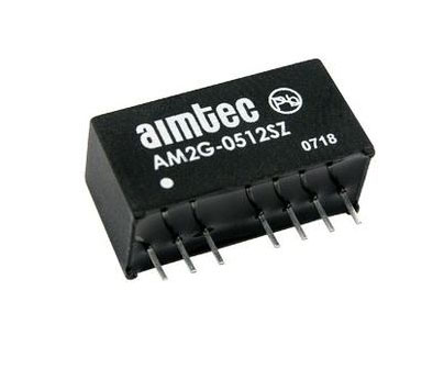 12V DC-DC Converter AM2G-0512SZ: Specifications, Datasheet, Applications and Features6/3/2024 638
A DC-DC converter is an essential electronic device to convert a direct current (DC) source from one voltage level to another. These converters are widely employed in various applications, including portable electronic devices, automotive systems, and renewable energy installations.
Read More >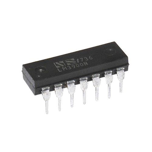 What is LM3900 Quadruple Norton Operational Amplifier?5/30/2024 1286
The LM3900 consists of four independent dual-input internally compensated amplifiers. These amplifiers are specifically designed to operate on a single power supply voltage and provide a large output voltage swing. They utilize current mirrors to achieve in-phase input functionality. Applications include AC amplifiers, RC active filters, low-frequency triangle waves, square wave, and pulse waveform generation circuits, tachometers, and low-speed, high-voltage digital logic gates.
Read More >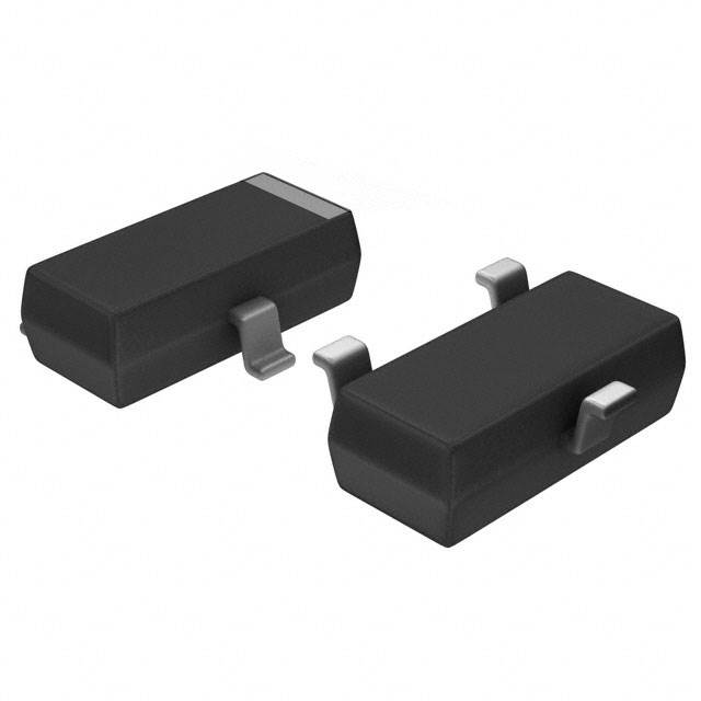 Exploring the MMBT3906 Transistor: A Comprehensive Guide5/24/2024 913
The goal of the Taiwan Semiconductor MMBT3906 PNP Bipolar Transistor is to provide a high surge current capability with minimal power loss. This transistor is perfect for automated installation and has high efficiency.
Read More >
SUPPORT
ABOUT BITFOIC
QUICK LINKS
Connect with us
Tel: 86-755-23606554
E-mail: [email protected]
Address: Room A29, 24 / F, Hoi Tak Wai, Prince Edward industrial building, 706 Prince Edward Road East, San Po Kong, Kowloon,Hongkong
Mon-Fri: 09.30 AM - 18.30 PM


