


NE555 VS LM555: What is the difference and which one is better?
Introduction
The NE555 and LM555 are popular timer ICs (integrated circuits) widely used in electronic circuits for generating precise time delays, oscillations, and pulse-width modulation. Developed by Signetics and National Semiconductor, these ICs have similar functionality but differ in some key aspects. This article explores the NE555 vs LM555 debate, highlighting their features, differences, and considerations for choosing the right timer IC for your project.
Table of Content
1. What is NEE555?
NE555 is a medium-scale integrated device that combines analog and digital functions. This chip has multiple functions and can be used as a timer, oscillator, and pulse generation circuit.
Engineers today still use the 555 to design some useful electronic modules, mainly because the integrated chip made from a single crystal is as reliable and cheap as an operational amplifier circuit. It can produce a stable square wave signal with a duty cycle from 50% to 100%. , 555 has low cost and reliable performance.
Only a few external resistors and capacitors are needed to realize pulse generation and conversion circuits such as multiple oscillator monostable triggers and Schmitt triggers.
NE555 is also often used as a timer and is widely used in instrumentation, household appliances, electronic measurement, and automatic control. It is now the first choice among thousands of application solutions. The applications of 555 can be classified according to their working mode into none. Stable monostable bistable.
Another very important point is that it can generate PWM waveforms. For example, its application can be seen in switching power supply circuits, thanks to its low price and its ability to be well combined with other circuits.
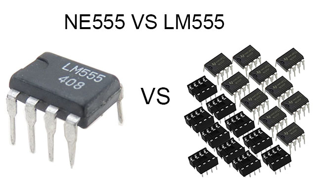
Figure1-NE555 VS LM555
2. What is LM555?
The LM555 is a highly stable device for generating accurate time delays or oscillations. Additional terminals are provided for triggering or resetting if desired. In the time delay mode of operation, the time is precisely controlled by one external resistor and capacitor. For a stable operation as an oscillator, the free-running frequency and duty cycle are accurately controlled with two external resistors and one capacitor. The circuit may be triggered and reset on falling waveforms, and the output circuit can source or sink up to 200 mA or drive TTL circuits.
3. LM555 Features
- Directly replace SE555/NE555.
- Timing time ranges from microseconds to hours.
- Work in both astable and monostable modes.
- Adjustable duty cycle.
- The output can receive and source 200mA.
- The output voltage is compatible with TTL levels.
- Temperature stability is better than 0.005%/℃.
4. Pinout: LM555 VS NE555
4.1 LM555 Pinout
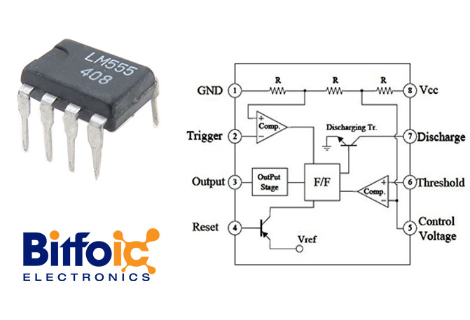
Figure2-Pinout: NE555 VS LM555
The LM555 time base circuit is internally composed of a voltage divider, a comparator, a flip-flop, an output tube, a discharge tube, etc. It is a mixture of analog circuits and digital circuits. Among them, pin 6 is the threshold terminal (TH), which is the input of the upper comparator. Pin 2 is the trigger terminal (TR), which is the input of the lower comparator. Pin 3 is the output terminal (OUT), which has two states: 0 and 1. Its state is determined by the level applied to the input terminal. Pin 7 is the discharge terminal (DIS), which is the output of the internal discharge tube. It has two states: floating and grounded, and is also determined by the state of the input terminal. Pin 4 is the reset terminal (R), which can cause the output terminal to be at a low level when the voltage is raised to a low level (< 0.3V). Pin 5 is the control voltage terminal (CV), which can be used to change the upper and lower trigger level values. Pin 8 is the power supply (VCC) and pin 1 is the ground (GND).
Generally, the LM555 circuit can be equivalent to an R-S flip-flop of a large discharge switch. This special flip-flop has two input terminals: the threshold terminal (TH) can be regarded as the zero-setting terminal R, which requires a high level; the trigger terminal (TR) can be regarded as the setting terminal S, which is effective at a low level. It has only one output terminal OUT, which can be equivalent to the Q terminal of the flip-flop. The discharge terminal (DIS) can be regarded as a contact controlled by the internal discharge switch. The discharge switch is controlled by the inverse Q terminal of the flip-flop: when inverse Q=1, the DIS terminal is grounded; when inverse Q=0, the DIS terminal is suspended. In addition, this flip-flop has a reset terminal R, a control voltage terminal CV, a power supply terminal VCC, and a ground terminal GND.
This special R-S flip-flop has two characteristics: (1) The trigger level of the two input terminals requires one high and one low: the zero-setting terminal R, which is the threshold terminal TH, requires a high level, and the set terminal S, which is the trigger terminal TR A low level is required. (2) The trigger levels of the two input terminals, that is, the threshold voltage values that cause them to flip are also different. When the CV terminal is not connected to the control voltage, for the TH (R) terminal, > 2/3VCC is high level 1. " 2/3VCC is low level 0; and for the TR (S) terminal, " 1/3VCC is high level 1, " 1/3VCC is low level 0. If the control voltage VC is added to the control terminal CV, the upper trigger level becomes the VC value, and the lower trigger level becomes 1/2VC. It can be seen that changing the control voltage value of the control terminal can change the upper and lower trigger level values.
4.2 NE555 Pinout
The function of the 555 timer is mainly determined by two comparators. The output voltages of the two comparators control the state of the RS flip-flop and the discharge tube. Add a voltage between the power supply and the ground. When pin 5 is left floating, the voltage at the non-inverting input terminal of voltage comparator C1 is 2VCC /3, and the voltage at the inverting input terminal of C2 is VCC /3. If the voltage of the trigger input terminal TR is less than VCC /3, the output of the comparator C2 is 0, which can set the RS flip-flop to 1 and make the output terminal OUT=1. If the voltage of the threshold input terminal TH is greater than 2VCC/3, and the voltage of the TR terminal is greater than VCC /3, then the output of C1 is 0 and the output of C2 is 1. The RS flip-flop can be set to 0 to make the output low level.
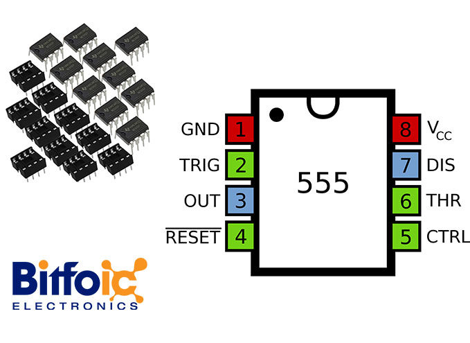
Figure3-Pinout: NE555 Pinout
Pin functions are as follows:
Pin 1: The negative terminal of the external power supply is VSS or ground, which is usually grounded.
Pin 2: low trigger terminal TR.
Pin 3: Output Vo
Pin 4: It is the direct clearing terminal. When this terminal is connected to a low level, the time-base circuit will not work. At this time, no matter what level TR and TH are at, the output of the time base circuit is "0". When this terminal is not used, it should be connected to a high level.
Pin 5: VC is the control voltage terminal. If this terminal is connected to an external voltage, the reference voltage of the two internal comparators can be changed. When this terminal is not in use, a 0.01μF capacitor should be connected to this terminal in series to ground to prevent interference.
Pin 6: High trigger terminal TH.
Pin 7: Discharge terminal. This end is connected to the collector of the discharge tube and is used to discharge the capacitor when used as a timer.
Pin 8: External power supply VCC. The range of VCC for a bipolar time base circuit is 4.5 ~ 16V, and the range of VCC for a CMOS time base circuit is 3 ~ 18V. Generally use 5V. When pin 1 is connected to the ground, pin 5 is not connected to an external voltage, and the reference voltages of the two comparators A1 and A2 are low level respectively, the function table of the 555-time base circuit is as shown in Table 1.
|
Table 1: Function table of 555 timer |
|||||
|
Clear terminal |
High trigger terminal TH |
Low trigger terminal TR |
V0 |
Discharge tube T(V) |
Function |
|
0 |
x |
x |
0 |
conduction |
Clear directly |
|
1 |
0 |
1 |
x |
keep the previous state |
keep the previous state |
|
1 |
1 |
0 |
1 |
Deadline |
Set to 1 |
|
1 |
0 |
0 |
1 |
Deadline |
Set to 1 |
|
1 |
1 |
1 |
0 |
conduction |
Clear |
5. Internal Circuit: LM555 VS NE555
Since most second-source chips are sold as "plug-in" replacements for the original chips, few people notice that the internals of the chip may have been modified a bit, but luckily the manufacturer has added a (Simplified) schematic, we will explore this.
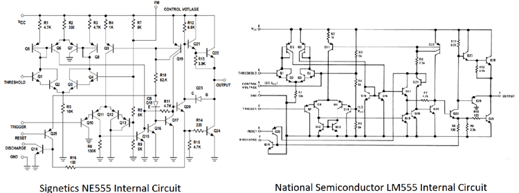
Figure4-Internal Circuit
The use of current mirror active loads in the LM555 is one of the most significant differences between the two chips.
6. LM555 VS NE555: What is the difference in circuit application?
Although "pin" compatible, the changes in the LM555 make the circuit behave very differently compared to the NE555.
As we know from the internal diagram, in LM555 we replace the fixed resistor with an active load. One of the main benefits of switching from resistive to active loads is that it reduces the dependence of output timing on temperature and supply voltage.
This is highlighted in Signetics' NE555 original datasheet.
Another difference is that in the original NE555, the trigger signal was given higher priority, while in the LM555, the threshold signal was given higher priority.
Normally, in a 555 timer, when pin 2 (trigger) is below 1/3VCC, the output goes high, and when pin 6 (threshold) is above 2/3VCC, the output goes low.
In NE555, if the trigger pin goes low, the output will go low even if the threshold pin is high.
However, in LM555, the output remains low even if the trigger pin goes low, and only when the threshold pin goes low, does the output go high again.
There have been reports of extra unwanted pulses on the output of the LM555, possibly due to different priorities assigned to the threshold and trigger pins.
7. Manufacturer: LM555 VS NE555
Different manufacturers have the same model. The prefix of an integrated circuit represents the manufacturer, the middle number is the model code, and the suffix generally represents temperature, packaging, and other characteristics.
The functions of NE555 and LM555 are the same, except that the former was originally produced by Japan's NEC Company. In contrast, LM was first produced by the National Semiconductor Company of the United States.
8. LM555 VS NE555: Which one is better?
LM555 and NE555 are counters, regardless of accuracy, their speed is the same, and other indicators are similar.
The better one is TLC555, which is much faster than LM555 and NE555 but consumes much less power.
Conclusion
From the above description, we can conclude that the main difference between NE555 and LM555 is that the NE555 output timing depends on temperature and supply voltage, and the trigger pin has a higher priority. However, the LM555 output timing is relatively independent of temperature and supply voltage, and the threshold pin has a higher priority.
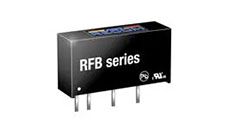 DC-DC converter RFB-0505S: Specification,Datasheet,Features and Applications6/13/2024 555
The RFB-0505S is a DC-DC converter from RECOM Power, Inc., belonging to the RFB Series. It features a Single In-Line Package (SIP7) and provides a single unregulated output. This converter offers 1 watt of power with an output voltage of 5V and is rated for an isolation voltage of 1kV.
Read More >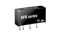 Understanding the RFMM-0505S DC-DC Converter: A Comprehensive Guide6/4/2024 730
In the world of electronics, ensuring efficient power management is crucial for the performance and reliability of devices. One of the key components in achieving this is the DC-DC converter. Today, we dive into the specifics of the RFMM-0505S DC-DC converter, exploring its features, applications, and benefits.
Read More >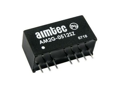 12V DC-DC Converter AM2G-0512SZ: Specifications, Datasheet, Applications and Features6/3/2024 654
A DC-DC converter is an essential electronic device to convert a direct current (DC) source from one voltage level to another. These converters are widely employed in various applications, including portable electronic devices, automotive systems, and renewable energy installations.
Read More >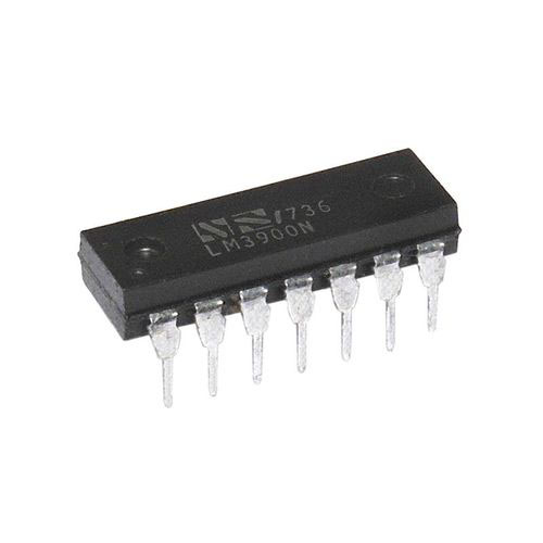 What is LM3900 Quadruple Norton Operational Amplifier?5/30/2024 1307
The LM3900 consists of four independent dual-input internally compensated amplifiers. These amplifiers are specifically designed to operate on a single power supply voltage and provide a large output voltage swing. They utilize current mirrors to achieve in-phase input functionality. Applications include AC amplifiers, RC active filters, low-frequency triangle waves, square wave, and pulse waveform generation circuits, tachometers, and low-speed, high-voltage digital logic gates.
Read More > Exploring the MMBT3906 Transistor: A Comprehensive Guide5/24/2024 931
The goal of the Taiwan Semiconductor MMBT3906 PNP Bipolar Transistor is to provide a high surge current capability with minimal power loss. This transistor is perfect for automated installation and has high efficiency.
Read More >
SUPPORT
ABOUT BITFOIC
QUICK LINKS
Connect with us
Tel: 86-755-23606554
E-mail: [email protected]
Address: Room A29, 24 / F, Hoi Tak Wai, Prince Edward industrial building, 706 Prince Edward Road East, San Po Kong, Kowloon,Hongkong
Mon-Fri: 09.30 AM - 18.30 PM


