


LP2985-33DBVR low-dropout regulators: Pinout, Pin Configuration, Datasheet, CAD Model, Specification, Applications and Features.
Introduction
The LP2985 series of fixed output, low-dropout regulators provide excellent, cost-effective performance for portable and non-portable applications. This post can help you learn its pinout and configuration as well as CAD model, specification, applications, and features.
Catalog
ⅢLP2985 LDO Pinout Configuration
Ⅷ LP2985 Functional Block Diagram
XIII Dropout Voltage vs Temperature for New Chip
XV LP2985 Frequently Asked Questions
ⅠLP2985 Description
The LP2985 is a fixed-output, wide-input, low-noise, low-dropout voltage regulator supporting an input voltage range from 2.5 V to 16 V and up to 150 mA of load current. The LP2985 supports an output range of 1.2 V to 5.0 V (for a new chip). LP2985 has an Enable pin to provide Zero-current shutdown mode. This voltage regulator comes with features, such as overcurrent and over-temperature protection.
Ⅱ LP2985 Pinout
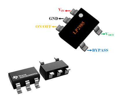
Figure1-LP2985 Pinout
Ⅲ LP2985 LDO Pinout Configuration
|
Pin No. |
Pin Name |
Description |
|
1 |
VIN |
Supply Input |
|
2 |
GND |
Ground |
|
3 |
ON/OFF |
Active-low shutdown pin. Logic-high = enable, logic-low or open = shutdown |
|
4 |
BYP |
Reference Bypass: Connect the external 470 pF capacitor to GND to reduce output noise. May be left open. |
|
5 |
OUT |
Regulator Output |
Ⅳ LP2985 Features
- VINrange (new chip): 2.5 V to 16 V
- VOUTrange (new chip): 1.2 V to 5.0 V (fixed, 100-mV steps)
- VOUTaccuracy:
- ±1% for A-grade legacy chip
- ±1.5% for standard-grade legacy chip
- ±0.5% for new chip only
- ±1% output accuracy over load, and temperature for new chip
- Output current: Up to 150 mA
- Low IQ(new chip): 71 µA at ILOAD = 0 mA
- Low IQ(new chip): 750 µA at ILOAD = 150 mA
- Shutdown current:
- 01 µA (typ) for legacy chip
- 12 µA (typ) for new chip
- Low noise: 30 µVRMSwith 10-nF bypass capacitor
- Output current limiting and thermal protection
- Stable with 2.2-µF ceramic capacitors
- High PSRR: 70 dB at 1 kHz, 40 dB at 1 MHz
- Operating junction temperature: –40°C to +125°C
- Package: 5-pin SOT-23 (DBV)
Ⅴ LP2985-33DBVR CAD Model
LP2985-33DBVR Symbol

Figure2-LP2985-33DBVR Symbol
LP2985-33DBVR Footprint
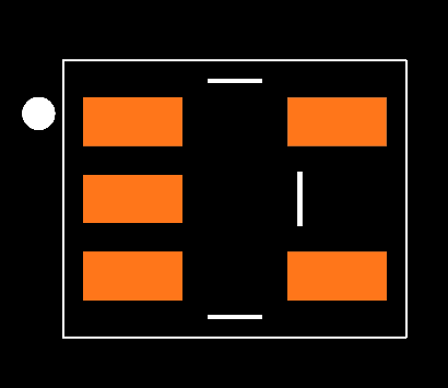
Figure3-LP2985-33DBVR footprint
LP2985-33DBVR 3D Model
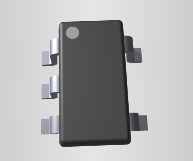
Figure4-LP2985-33DBVR 3d model
Ⅵ LP2985 Parameters
|
Output options |
Fixed Output |
|
Iout (Max) (A) |
0.15 |
|
Vin (Max) (V) |
16 |
|
Vin (Min) (V) |
2.2 |
|
Vout (Max) (V) |
10 |
|
Vout (Min) (V) |
1.8 |
|
Fixed output options (V) |
1.8, 2.5, 2.8, 2.9, 3, 3.3, 5, 10 |
|
Noise (uVrms) |
30 |
|
Iq (Typ) (mA) |
0.065 |
|
Thermal resistance θJA (°C/W) |
206 |
|
Rating |
Catalog |
|
Load capacitance (Min) (µF) |
2.2 |
|
Regulated outputs (#) |
Enable |
|
Accuracy (%) |
5 |
|
PSRR @ 100 KHz (dB) |
40 |
|
Dropout voltage (Vdo) (Typ) (mV) |
280 |
|
Operating temperature range (C) |
-40 to 125 |
Ⅶ LP2985 Equivalents
MIC5205, TPS73633, TLV713
Ⅷ LP2985 Functional Block Diagram

Figure5-LP2985 Functional Block Diagram
Ⅸ LP2985 Layout Example
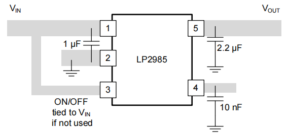
Figure6-LP2985 layout example
LP2985 is specially designed for Portable Devices, Digital Cameras, and MP3 players by Texas Instruments. The input voltage of the Regulator can be between 2.2V to 16V, the LP2985 includes a CMOS or TTL-compatible enable/shutdown control input. When shutting down, power consumption drops nearly to zero. Output noise in LP2985 is further reduced by the bypass pin. The functional block diagram of LP2985 is shown below. The main components of this regulator are the Reference voltage, Error amplifier, and Pass element (transistor).
Ⅹ How to use the LP2985 LDO
LP2985 low dropout regulator comes in a 5-pin package. In the LP2985 regulator, an extra bypass pin is introduced for further output noise reduction. This pin is connected to the ground through an optional 10nf capacitor. A Vin pin is connected to the input power supply and a 1µf ceramic capacitor is used for input noise cancellation. The regulated voltage is obtained from the Vout pin. Enable pin can be used to turn on or off the regulator, this helps the designers to turn off the regulator and prevent battery usage when not in use. The application diagram for the LP2985 voltage regulator is shown below.
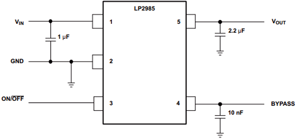
Figure7-how to use LP2985 LDO
Ⅺ Applications
- Portable Devices
- Digital Cameras and Camcorders
- CD Players
- MP3 Players
Typical Application Circuit
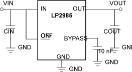
Figure8-Typical Application Circuit
Ⅻ LP2985 Package
Dimensions for the LP2985 Voltage Regulator are given below.
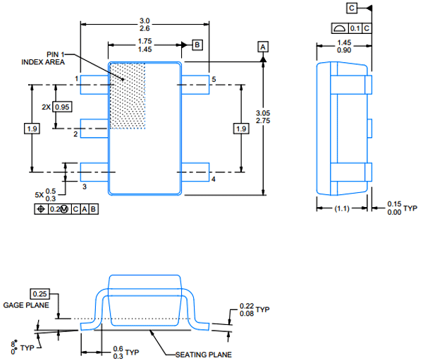
Figure9-LP2985 Package
XIII Dropout Voltage vs Temperature for New Chip
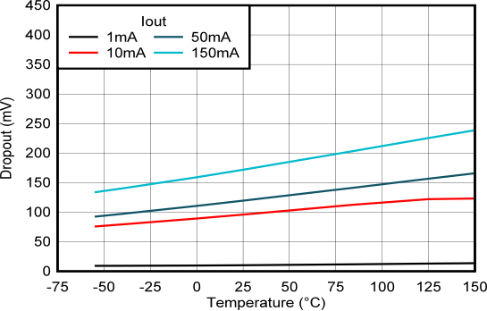
Figure10-Dropout Voltage vs Temperature for New Chip
XIV LP2985 Datasheet PDF
 DC-DC converter RFB-0505S: Specification,Datasheet,Features and Applications6/13/2024 504
The RFB-0505S is a DC-DC converter from RECOM Power, Inc., belonging to the RFB Series. It features a Single In-Line Package (SIP7) and provides a single unregulated output. This converter offers 1 watt of power with an output voltage of 5V and is rated for an isolation voltage of 1kV.
Read More > Understanding the RFMM-0505S DC-DC Converter: A Comprehensive Guide6/4/2024 686
In the world of electronics, ensuring efficient power management is crucial for the performance and reliability of devices. One of the key components in achieving this is the DC-DC converter. Today, we dive into the specifics of the RFMM-0505S DC-DC converter, exploring its features, applications, and benefits.
Read More >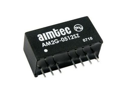 12V DC-DC Converter AM2G-0512SZ: Specifications, Datasheet, Applications and Features6/3/2024 607
A DC-DC converter is an essential electronic device to convert a direct current (DC) source from one voltage level to another. These converters are widely employed in various applications, including portable electronic devices, automotive systems, and renewable energy installations.
Read More >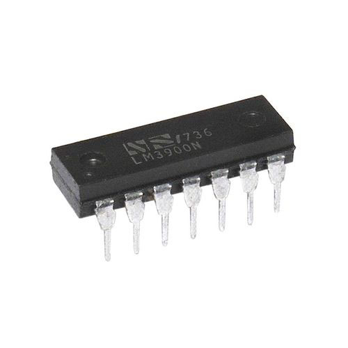 What is LM3900 Quadruple Norton Operational Amplifier?5/30/2024 1218
The LM3900 consists of four independent dual-input internally compensated amplifiers. These amplifiers are specifically designed to operate on a single power supply voltage and provide a large output voltage swing. They utilize current mirrors to achieve in-phase input functionality. Applications include AC amplifiers, RC active filters, low-frequency triangle waves, square wave, and pulse waveform generation circuits, tachometers, and low-speed, high-voltage digital logic gates.
Read More >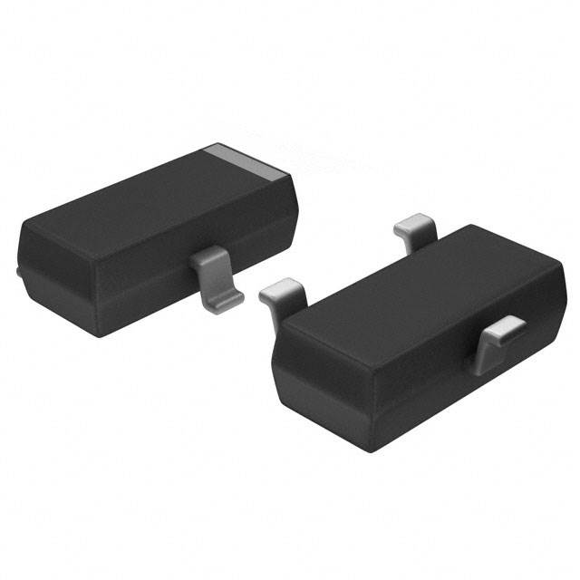 Exploring the MMBT3906 Transistor: A Comprehensive Guide5/24/2024 865
The goal of the Taiwan Semiconductor MMBT3906 PNP Bipolar Transistor is to provide a high surge current capability with minimal power loss. This transistor is perfect for automated installation and has high efficiency.
Read More >
SUPPORT
ABOUT BITFOIC
QUICK LINKS
Connect with us
Tel: 86-755-23606554
E-mail: [email protected]
Address: Room A29, 24 / F, Hoi Tak Wai, Prince Edward industrial building, 706 Prince Edward Road East, San Po Kong, Kowloon,Hongkong
Mon-Fri: 09.30 AM - 18.30 PM


