


LM1117 voltage regulator: Pinout, Features, Specifications, Circuits and Applications
Introduction
We often use various types of electrical, electronic, and mechanical devices to meet our daily needs, but the functionality and the required power requirements of these devices are different. The power supplied to these devices sometimes fluctuates for various reasons. Some of these can withstand fluctuations in power, while others may damage the device. To prevent damage to devices caused by unstable power supplies, a device that can provide a stable output voltage even if the input voltage changes is needed, that is, a voltage regulator. In this article, we will briefly introduce a linear voltage regulator-LM1117.
Table of Content
1. What is LM1117?
The LM1117 is an adjustable voltage regulator that provides fixed and variable voltages.
First, fixed voltages of 1.8, 2.5, 2.85, 3.3, and 5V are available. Best of all, we can set it in the range of 1.25 to 13.8 V with an adjustable output voltage.
This regulator can regulate the input voltage even if it is close to the supply voltage, and it has built-in thermal and current limit protection.
Figure1-LM1117
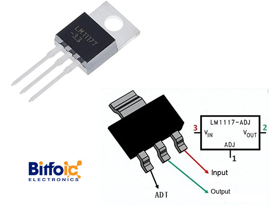
2. LM1117 Pinout and pin configuration
LM1117 has 4 different packages from different manufacturers including DCY package 4-pin SOT, KTT package 3-pin TO-263, NDE package 3-pin TO-220, NDP package 3-pin TO-252, NGN package 8-pin WSON. There are three main pins on the LM1117 package – input pin, output pin, and ground pin. In all the above packages, pin 1 worked as a ground pin in fixed voltage mode and an adjustable pin in adjustable mode.
LM1117 Pinout
Pin 3 in all packages except WSON is the input voltage pin for the regulator VIN. In the WSON package, pins 2, 3, and 4 are input pins of the voltage regulator. Pin 2 and TAB of all packages except WSON worked as the output voltage pin of the regulator VOUT.
In the WSON package, pins 5, 6, 7, and TAB, and in package SOT-223, pins 2 and 4 are output pins of the voltage regulator. When using the WSON package, pins 2, 3, and 4 should be connected, and pins 5, 6, and 7 should be connected.
LM117 pinout
Pin Configuration
|
Pin Number |
Pin name |
Description |
|
1 |
Adjust/Ground |
Adapt/Set Aside This pin modifies the output voltage and serves as ground if the voltage regulator is fixed.
|
|
2 |
Output Voltage(Vout) |
Two-Voltage Output (Vout) This pin provides access to the controlled output voltage that the adjust pin has set.
|
|
3 |
Input Voltage (Vin) |
The input voltage which has to be regulated is given to this pin
|
3. LM1117 Features
- losing To-220, SOT223, TO263 packaging
- linear voltage regulator with a minimum voltage drop of 1.1V
- generates fixed voltages of 1.8, 2.5, 3.3, and 5 V
- the variable voltage range is 1.25V to 13.8V
- The maximum input voltage of this IC is 20V
- the operating junction temperature is 125 °C
- maximum 0.1% line regulation and maximum 0.2% load regulation
- The output current is 800mA
- built-in thermal protection circuit to prevent IC from overheating
- provide over-current protection
4. LM1117 Specifications
The specifications of LM1117 are mainly reflected in the following aspects:
- Work at 0°C to 120°C.
- The maximum input voltage is 20V.
- power consumption is limited internally.
- With current limiting and thermal protection circuit.
- electrostatic discharge is ±2000v.
- has a minimum dropout voltage of 1.1V.
- The minimum load current for the adjustable LM1117 operating at 250°C and 15V input voltage is 1.7mA. The current is 5mA when operating over 0 to 125°C.
- Thermal regulation at 250°C is a minimum of 0.01/%w.
- To protect the regulator from thermal effects, an external diode is connected between the input and output pins.
- These have a maximum line regulation of 0.1%.
- The maximum load regulation rate provided is 0.2%.
- With level 3 humidity sensitivity.
- storage temperature range is - 65C to 150°C.
5. LM1117 voltage stabilization principle
5.1 LM1117 Internal block diagram
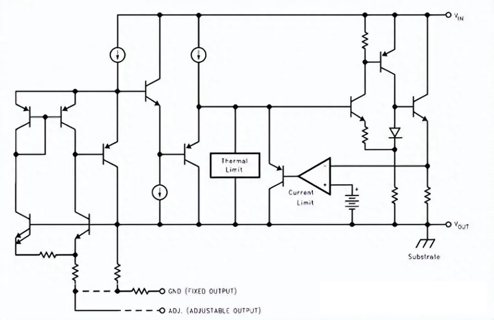
LM1117 internal block diagram
5.2 LM1117 Voltage stabilization principle
We can understand LM117 circuits by looking at the basic circuit of a low dropout linear regulator. It consists of a differential amplifier, FETs, and resistors. This series uses Zener diodes with cut-off voltage VZ.
LM1117 circuit
The reference voltage applied to the differential amplifier is also equal to VZ. The input should be greater than the sum of the output voltage and the dropout value to keep the regulator in working condition.
It comes in two types:
- Adjustable form in which the output voltage of the regulator can be adjusted with the help of two external resistors.
- Fixed voltage form, in which the output voltage of the regulator is a fixed value. The LM1117 is available in fixed voltage versions in 1.8V, 2.5V, 3.3V and 5V ranges.
In circuits, capacitors can filter out noise from signals. Capacitors are used at both the input and output ends, and the value of the capacitor can be chosen as desired, but generally, the capacitor at the input end has a higher value than the capacitance at the output end. 10UF is the minimum value of the capacitor used at the output.
Input voltage controls the source of the FET circuit. The differential amplifier controls the gate of the FET circuit. When the input voltage is less than the sum of the output voltage and dropout voltage, the differential amplifier causes the FET gate value to be zero. In this case, the FET behaves as a simple resistor circuit with the input value equal to the output value
6. How to use LM1117?
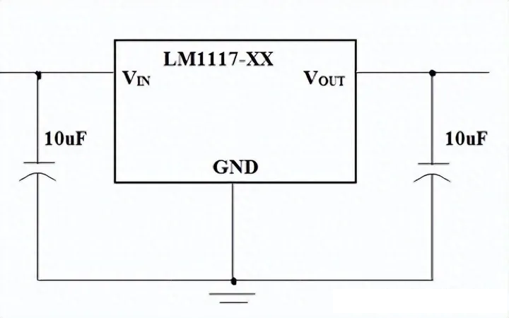
The LM1117 is a simple device to use. If the IC has a fixed voltage regulator, the Vin pin can power it and the Vout pin gets a regulated output. In this case, the Adj/Ground pin is used only as a ground pin and is connected to the ground. To filter out noise, a capacitor can be placed on the output side.
The circuit diagram of a fixed output regulator is given below.

fixed output regulator circuit
In this circuit, capacitors connect to the input and output. They carry out the task of removing noise from the voltage signal output. The minimum value of the capacitor used at the output is 10µF, but the input capacitor is usually higher in value than the output capacitor. Output capacitor provides stable voltage and improves transient response.
7. LM1117 Typical Application Circuits
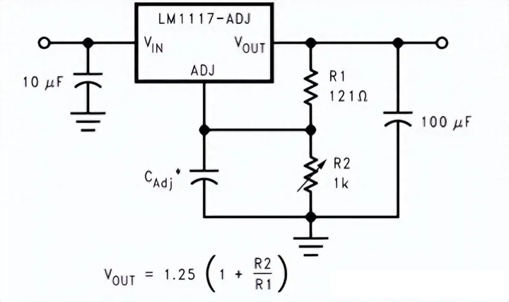
variable output voltage circuit
This adjustable voltage regulator also provides adjustable voltage from 12.5 to 13.8 V. The adjustable output circuit is shown in the figure below.
It works by generating a 1.25 V reference voltage through the output and trim pins. We apply this reference voltage across resistor R1.
Resistor R1 produces constant current I1. I1 will flow through R2 because the two resistors are connected in parallel. This current will then produce the desired output voltage. Two resistors R1 and R2 are used to set the desired voltage. The formula for finding the voltage through any of these registers is:
Vout = 1.25 (1 + R2/R1).
variable output voltage circuit
Bypass capacitor function: The bypass capacitor Cadj is connected to the adjustable pin to improve ripple suppression. As the output voltage increases, the ripple will be amplified. Therefore, this capacitor can prevent the ripple from being amplified. In some applications, an external diode is connected between the input pin and the output pin to protect the regulator from thermal effects.
8. Applications
- Used for Positive voltage regulations
- Variable power supply
- Current limiting circuits
- Reverse polarity circuits
- Often utilized in desktop computers, DVDs, and more consumer goods
- Used in motor control circuits
9. 2D – Model of LM1117 (DCY Package)
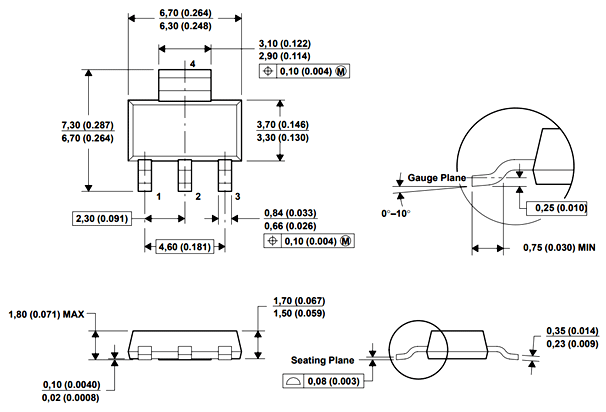
2D – Model of LM1117 (DCY Package)
 DC-DC converter RFB-0505S: Specification,Datasheet,Features and Applications6/13/2024 577
The RFB-0505S is a DC-DC converter from RECOM Power, Inc., belonging to the RFB Series. It features a Single In-Line Package (SIP7) and provides a single unregulated output. This converter offers 1 watt of power with an output voltage of 5V and is rated for an isolation voltage of 1kV.
Read More > Understanding the RFMM-0505S DC-DC Converter: A Comprehensive Guide6/4/2024 758
In the world of electronics, ensuring efficient power management is crucial for the performance and reliability of devices. One of the key components in achieving this is the DC-DC converter. Today, we dive into the specifics of the RFMM-0505S DC-DC converter, exploring its features, applications, and benefits.
Read More >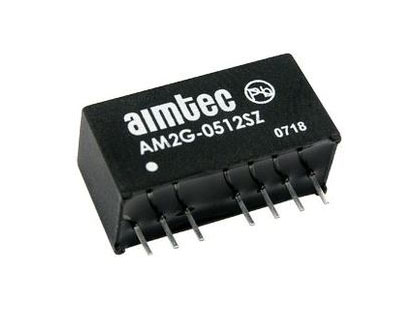 12V DC-DC Converter AM2G-0512SZ: Specifications, Datasheet, Applications and Features6/3/2024 671
A DC-DC converter is an essential electronic device to convert a direct current (DC) source from one voltage level to another. These converters are widely employed in various applications, including portable electronic devices, automotive systems, and renewable energy installations.
Read More >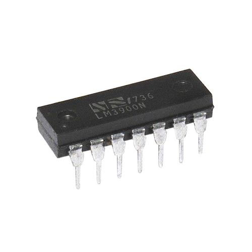 What is LM3900 Quadruple Norton Operational Amplifier?5/30/2024 1347
The LM3900 consists of four independent dual-input internally compensated amplifiers. These amplifiers are specifically designed to operate on a single power supply voltage and provide a large output voltage swing. They utilize current mirrors to achieve in-phase input functionality. Applications include AC amplifiers, RC active filters, low-frequency triangle waves, square wave, and pulse waveform generation circuits, tachometers, and low-speed, high-voltage digital logic gates.
Read More > Exploring the MMBT3906 Transistor: A Comprehensive Guide5/24/2024 963
The goal of the Taiwan Semiconductor MMBT3906 PNP Bipolar Transistor is to provide a high surge current capability with minimal power loss. This transistor is perfect for automated installation and has high efficiency.
Read More >
SUPPORT
ABOUT BITFOIC
QUICK LINKS
Connect with us
Tel: 86-755-23606554
E-mail: [email protected]
Address: Room A29, 24 / F, Hoi Tak Wai, Prince Edward industrial building, 706 Prince Edward Road East, San Po Kong, Kowloon,Hongkong
Mon-Fri: 09.30 AM - 18.30 PM


