


CD4007 CMOS Inverter: Pinout, Datasheet, Circuits, Features and Applications[FAQ&Video]
Introduction
CD4007 is a dual complementary pair plus inverter. This page will introduce details about the CD4007 inverter, including its pin, features, applications, datasheet, etc.
Current Mirror Circuit using CD4007 in a Laboratory Setting
Catalog
Ⅰ What is CD4007?
The CD4007M/CD4007C consists of three complementary pairs of N- and P-channel enhancement mode MOS transistors suitable for series/shunt applications. The IC works in a variety of environments and connects directly to CMOS, NMOS, and TTL devices. The IC provides a wide range of applications, including strong noise immunity and low thermal dissipation. All pin voltages must be restricted to remain between VSS and VDD at 0.3V at all times in order for the device to function properly. Clamping diodes are used at VD and VSS to provide static protection for all inputs.
Ⅱ What is an Inverter?
An inverter configuration inverts the input digital signal. An inverter always has high or logic level 1 output when its input is low or at logic level 0, and a low or logic level 0 output when the input is high or at logic level 1.
Ⅲ CD4007 Pinout
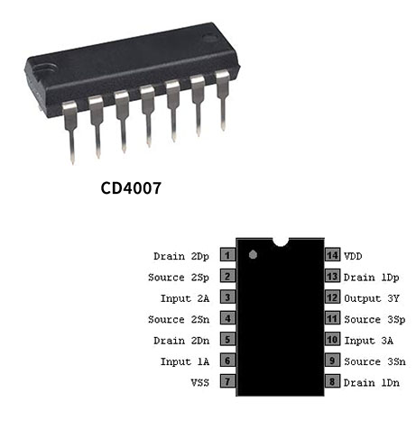
Figure1-CD4007 Pinout
|
Pin No |
Pin Name |
Description |
|
1 |
2Dp |
The drain of p Channel 2 |
|
2 |
2Sp |
Source of p Channel 2 |
|
3 |
2A |
Input Channel 2 |
|
4 |
2sn |
Source of n Channel 2 |
|
5 |
2Dn |
Drain of n Channel 2 |
|
6 |
1A |
Input Channel 1 |
|
7 |
VSS |
Source Supply |
|
8 |
1Dn |
Drain of n Channel 1 |
|
9 |
3Sn |
Source of n Channel 3 |
|
10 |
3A |
Input Channel 3 |
|
11 |
3Sp |
Source of p Channel 3 |
|
12 |
3Y |
output |
|
13 |
1Dp |
Drain of p Channel 1 |
|
14 |
VDD |
Drain Supply |
Ⅳ CD4007 Features
- High-Voltage Type (20V Rating)
- Standardized Symmetrical Output Characteristics
- Medium Speed Operation
- tPHL, tPLH = 30 ns (typ) at 10V
- 100% Tested for Maximum Quiescent Current at 20V
- Meets All Requirements of JEDEC Tentative Stan-
dards No. 13B, “Standard Specifications for Descrip-
tion of “B” Series CMOS Devices”
- Maximum Input Current of 1μA at 18V Over Full Pack-
age-Temperature Range; 100nA at 18V and +25oC
Ⅴ CD4007 Applications
- Extremely High-Input Impedance Amplifiers
- Shapers
- Inverters
- Threshold Detector
- Linear Amplifiers
- Crystal Oscillators
Ⅵ CD4007 Connection Diagram

Figure2-CD4007 Connection Diagram
Ⅶ How to make inverters with the CD4007?
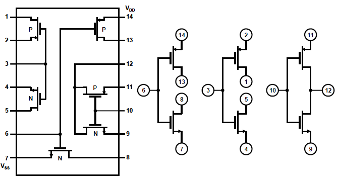
Figure3-schematic and pinout for the CD4007
Three individual inverters can be constructed from one CD4007 package.
Firstly, Connecting pins 8 and 13 together as the inverter output is the simplest configuration. The pin will be the input. Please confirm to connect pin 14VDD to power and pin 7 VSS to ground.
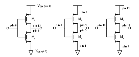
Figure4-CD4007 Inverter
Pins 2 and 4 are linked to VDD and VSS, respectively, pins 1 and 5 are connected as the output, and pin 3 is connected as the input to create the second inverter. Connecting pins 11 to VDD, 9 to VSS, 12 to be the output, and 10 to be the input creates the third inverter.
Ⅷ CD4007CM vs SN74HCT04DR vs MC14007UBD
|
Part Number |
|||
|
Manufacturer |
|||
|
Package / Case |
14-SOIC (0.154, 3.90mm Width) |
14-SOIC (0.154, 3.90mm Width)14-SOIC (0.154, 3.90mm Width) |
|
|
Number of Pins |
14 |
14 |
14 |
|
Logic Function |
Inverter |
|
Inverter |
|
Number of Circuits |
2 |
|
|
|
Number of Output Lines |
3 |
|
|
|
Propagation Delay |
50ns |
18ns |
55 ns |
|
Min Supply Voltage |
3 V |
|
3 V |
|
Supply Voltage |
3V ~ 15V |
5 V |
3V ~ 18V |
Ⅸ CD4007 Datasheet PDF
Ⅹ CD4007 Dimensions
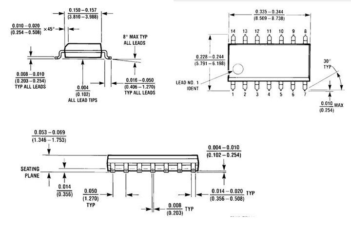
Figure5-CD4007 Dimensions
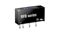 DC-DC converter RFB-0505S: Specification,Datasheet,Features and Applications6/13/2024 578
The RFB-0505S is a DC-DC converter from RECOM Power, Inc., belonging to the RFB Series. It features a Single In-Line Package (SIP7) and provides a single unregulated output. This converter offers 1 watt of power with an output voltage of 5V and is rated for an isolation voltage of 1kV.
Read More >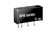 Understanding the RFMM-0505S DC-DC Converter: A Comprehensive Guide6/4/2024 758
In the world of electronics, ensuring efficient power management is crucial for the performance and reliability of devices. One of the key components in achieving this is the DC-DC converter. Today, we dive into the specifics of the RFMM-0505S DC-DC converter, exploring its features, applications, and benefits.
Read More >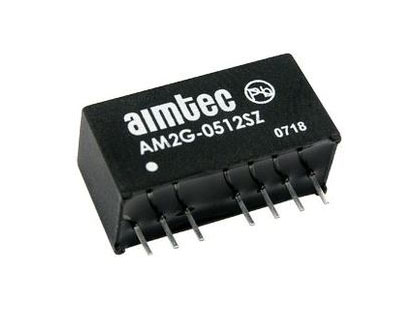 12V DC-DC Converter AM2G-0512SZ: Specifications, Datasheet, Applications and Features6/3/2024 671
A DC-DC converter is an essential electronic device to convert a direct current (DC) source from one voltage level to another. These converters are widely employed in various applications, including portable electronic devices, automotive systems, and renewable energy installations.
Read More >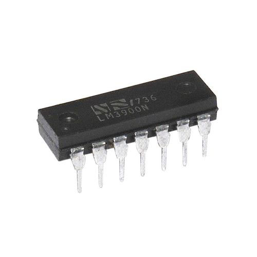 What is LM3900 Quadruple Norton Operational Amplifier?5/30/2024 1348
The LM3900 consists of four independent dual-input internally compensated amplifiers. These amplifiers are specifically designed to operate on a single power supply voltage and provide a large output voltage swing. They utilize current mirrors to achieve in-phase input functionality. Applications include AC amplifiers, RC active filters, low-frequency triangle waves, square wave, and pulse waveform generation circuits, tachometers, and low-speed, high-voltage digital logic gates.
Read More > Exploring the MMBT3906 Transistor: A Comprehensive Guide5/24/2024 966
The goal of the Taiwan Semiconductor MMBT3906 PNP Bipolar Transistor is to provide a high surge current capability with minimal power loss. This transistor is perfect for automated installation and has high efficiency.
Read More >
SUPPORT
ABOUT BITFOIC
QUICK LINKS
Connect with us
Tel: 86-755-23606554
E-mail: [email protected]
Address: Room A29, 24 / F, Hoi Tak Wai, Prince Edward industrial building, 706 Prince Edward Road East, San Po Kong, Kowloon,Hongkong
Mon-Fri: 09.30 AM - 18.30 PM


