


ATMega2560 Microcontroller: Features, Pinout, Comparisons, Datashheet and Arduino Mega 2560
Introduction
Atmega2560 is commonly found in the Arduino Mega 2560 as its main microcontroller. It’s an AVR RISC-based microcontroller that executes powerful instructions in a single clock cycle. This allows it to strike a fine balance between power consumption and processing speed.
In this blog, I’ll be covering Atmega2560 Features, pinout, Comparisons and datasheets.
Catalog
Ⅰ What is ATmega2560?
ATMega2560 is a low-power 8-bit microcontroller based on AVR-RISC architecture, which can execute effective instructions with a clock frequency of 16MHz. This microcontroller has 8KB SRAM, 4KB EEPROM and 256KB programmable flash memory with read and write functions. Of these, the bootloader uses 8KB of the 256KB flash memory.
ATmega2560 is designed for complex circuits and more storage, most electronic projects can be performed on other microcontrollers, which makes it uncommon, but very few projects can be done by ATmega2560 alone, because other microcontrollers Lack in terms of pins, storage and performance.
The ATmega2560 chip is primarily found in the Arduino Mega development board, which is useful in robotics projects that require a large number of GPIO pins.
Ⅱ ATMega2560 Pinout

Figure1-ATMega2560 Pinout
Ⅲ ATMega2560 Pin Configration
ATmega2560 has a total of 100 pins, 16 of which are analog input pins and 54 digital input/output pins. Of the 54 digital pins, 15 can be used as PWM pins. It also has 4 UART ports (8 pins), 5 SPI peripherals and 1 I2C port.
|
Pin Number |
Pin Name |
Description |
|
10, 31, 61, 80 |
VCC |
IC Supply pins |
|
11, 32, 62, 81, 99 |
GND |
IC ground reference pins |
|
98 |
AREF |
Reference supply for ADC |
|
100 |
AVCC |
Supply pin for analog peripherals |
|
33, 34 |
XTAL |
Crystal oscillator pins |
|
30 |
|
Reset pin, active low |
|
2 - 9 |
PE0 – PE7 |
GPIO Port E pins |
|
12 – 18, 27 |
PH0 – PH6, PH7 |
GPIO Port H pins |
|
19 - 26 |
PB0 – PB7 |
GPIO Port B pins |
|
28 – 29, 51 – 52, 70 |
PG3 – PG4, PG0 – PG1, PG2 |
GPIO Port G pins |
|
35 - 42 |
PL0 – PL7 |
GPIO Port L pins |
|
43 - 50 |
PD0 – PD7 |
GPIO Port D pins |
|
53 - 60 |
PC0 – PC7 |
GPIO Port C pins |
|
63 – 69, 79 |
PJ0 – PJ6, PJ7 |
GPIO Port J pins |
|
71 - 78 |
PA7 – PA0 |
GPIO Port A pins |
|
82 - 89 |
PK7 – PK0 |
GPIO Port K pins |
|
90 - 97 |
PF7 – PF0 |
GPIO Port F pins |
Ⅳ Features
- High Performance, Low Power AVR® 8-Bit Microcontroller
- Advanced RISC Architecture
- High Endurance Non-volatile Memory Segments
- QTouch® library support
- JTAG (IEEE® std. 1149.1 compliant) Interface
- Peripheral Features
- Special Microcontroller Features
- I/O and Packages
- Temperature Range:
-40°C to 85°C Industrial
- Ultra-Low Power Consumption
– Active Mode: 1MHz, 1.8V: 500µA
– Power-down Mode: 0.1µA at 1.8V
Other special features:
- Power-on Reset and Programmable Brown-out Detection
- Internal Calibrated Oscillator
- External and Internal Interrupt Sources
- Six Sleep Modes: Idle, ADC Noise Reduction, Power-save, Power-down, Standby, and Extended Standby
Ⅴ ATMega2560 Equivalents
Ⅵ ATMEGA2560 Applications
- Developing 3D printer.
- Controlling and handling more than one motor.
- Interfacing of a number of sensors.
- Sensing and detecting temperature.
- Water level detection projects.
- Home automation and security systems.
- Embedded Systems.
- IoT applications.
Ⅶ Block Diagram
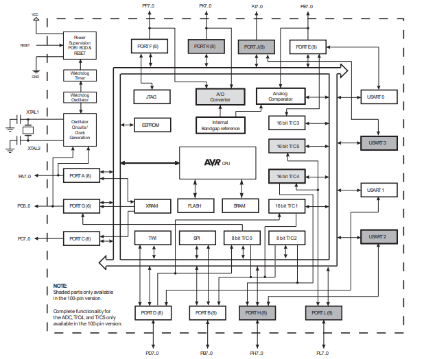
Figure 2-1. Block Diagram
The ATmega2560's AVR core combines a rich instruction set with 32 general-purpose working registers. All 32 registers are directly connected to the arithmetic logic unit (ALU). The resulting architecture is more code efficient and ten times faster than conventional CISC microcontrollers.
- CPU
To maximize performance, the Atmega2560 uses AVR-RISC (Harvard Architecture) – with separate memory and buses for program and data. As one instruction executes, the next instruction is prefetched from program memory. This concept enables instructions to be executed every clock cycle. Program memory is in-system reprogrammable flash memory.
- Logic unit
The ALU supports arithmetic and logical operations between registers or between constants and registers, and single-register operations can also be performed in the ALU.
- Memory
The ATmega2560 has two main memory spaces: data memory and program memory. In addition, ATmega2560 contains 256KB In-System
Reprogrammable Flash memory is used for program storage. For software security, the Flash Program storage space is divided into two parts: the Boot Program and the Application Program.
- Clock
ATmega2560 has many clocks, namely CPU clock, V/O clock, Flash clock, ADC clock, and asynchronous clock. None of the Atmega2560's clocks need to be active at a given time. To reduce power consumption, unused clock blocks can be stopped by using different sleep modes.
- Register
The ATmega2560 has 32 x 8-bit general-purpose working registers with a single clock cycle access time. Six of the 32 registers are available as three 16-bit indirect address register pointers for data space addressing, enabling efficient address computation.
- Communication peripherals
ATmega2560 provides 4 UART communication ports (TX-RX), 5 SPI peripherals, and 1 I2C peripheral.
- Operating parameters
The input voltage range of ATmega2560 is 2.7V-5.5V, and the output current of the input and output pins is close to about 40mA.
Ⅷ Microcontroller Comparisons
ATmega2560 belongs in an umbrella of microcontrollers; ATmega640/1280/1281/2560/2561. It does share common configurations such as the EEPROM and RAM but still consists of differences as shown below:
|
Device |
Flash |
General Purpose I/O pins |
16-bit resolution PWM channels |
Serial USARTs |
ADC Channels |
|
ATmega640 |
64KB |
86 |
12 |
4 |
16 |
|
ATmega1280 |
128KB |
86 |
12 |
4 |
16 |
|
ATmega1281 |
128KB |
54 |
6 |
2 |
8 |
|
ATmega2560 |
256KB |
86 |
12 |
4 |
16 |
|
ATmega2561 |
256KB |
54 |
6 |
2 |
8 |
The closest microcontroller that comes close to the ATmega2560 is the ATmega1280, with the only difference being the additional 128KB of flash.
Ⅸ How To Use ATMega2560?
It may be programmed using the Arduino development environment or another ATMega microcontroller with Atmel Studio, together with a specific programmer. The Arduino Mega board, which has the ATMega3560 and can be programmed by USB from the Arduino software, is the most user-friendly. Additionally, the GPIO pins are internally mapped to peripherals like SPI, USART, and SPI.Since the ATMega2560 operates on 5V logic levels, 3.3V sensors and other peripherals could not work with it. This is not a serious restriction because level-shifting circuits can get around it.
The ATMega2560 overcomes the restrictions of smaller microcontrollers like the ATMega328P and enables it to interface with more sensors and peripherals while still leaving a significant number of GPIO pins open for other tasks thanks to its large number of GPIO pins.
Ⅹ ATMEGA2560 Package
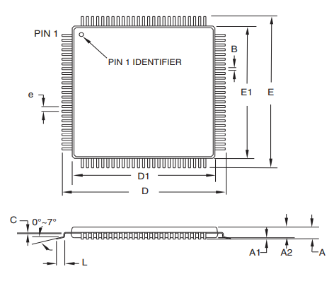
Figure3-package
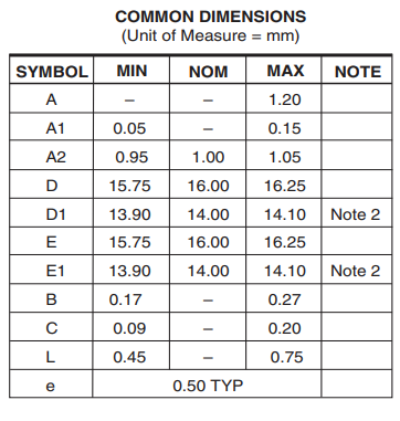
Figure4-package2
Ⅺ What is Arduino Mega 2560?
The Arduino Mega 2560 is a microcontroller board based on the ATmega2560. It has 54 digital input/output pins (of which 15 can be used as PWM outputs), 16 analog inputs, 4 UARTs (hardware serial ports), a 16 MHz crystal oscillator, a USB connection, a power jack, an ICSP header, and a reset button.
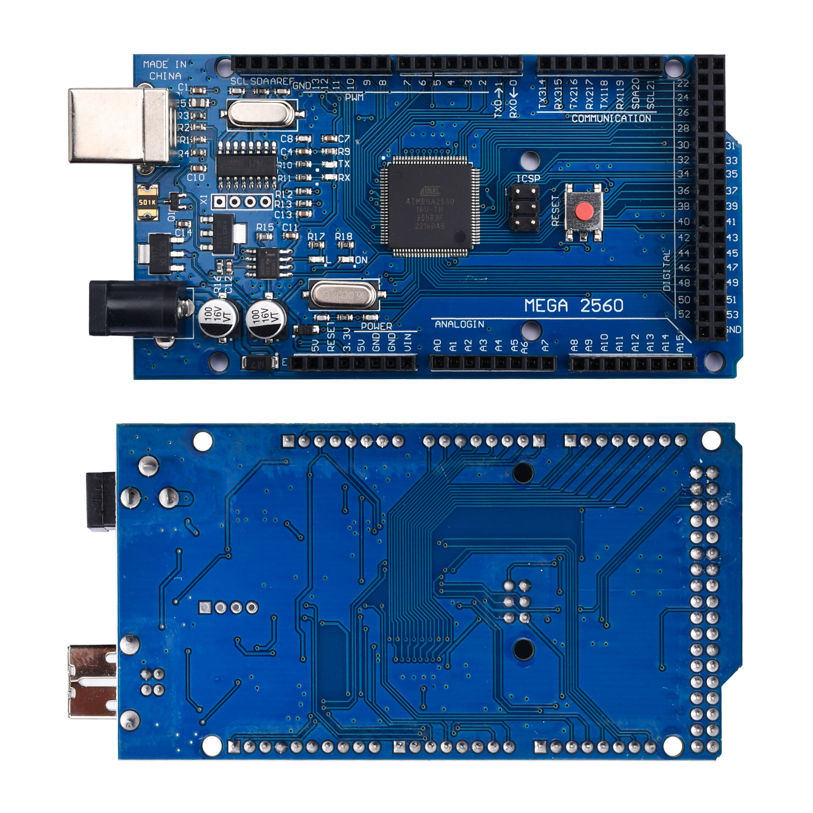
Figure5- Arduino Mega 2560
Known for its capabilities in handling more complex projects, the Arduino Mega 2560 gives your projects plenty of room and opportunities. It’s recommended for 3D printers and robotics projects with its 54 digital I/O pins, 16 analog inputs, and a large space.
Features/Specifications
- Operating voltage: 5V
- Input voltage (recommended): 7-12V
- Input voltage (limits): 6-20V
- Digital I/O pins: 54 (of which 14 provide PWM output)
- Analog input pins: 16
- DC current per I/O pin: 40mA
- DC current for 3.3V pin: 50mA
- Flash Memory: 256 KB, 8KB used by bootloader
- SRAM: 8 KB
- EEPROM: 4 KB
- Clock Speed: 16 MHz
Ⅻ ATMEGA2560 PDF
ATMEGA2560 Datasheet
 DC-DC converter RFB-0505S: Specification,Datasheet,Features and Applications6/13/2024 591
The RFB-0505S is a DC-DC converter from RECOM Power, Inc., belonging to the RFB Series. It features a Single In-Line Package (SIP7) and provides a single unregulated output. This converter offers 1 watt of power with an output voltage of 5V and is rated for an isolation voltage of 1kV.
Read More > Understanding the RFMM-0505S DC-DC Converter: A Comprehensive Guide6/4/2024 769
In the world of electronics, ensuring efficient power management is crucial for the performance and reliability of devices. One of the key components in achieving this is the DC-DC converter. Today, we dive into the specifics of the RFMM-0505S DC-DC converter, exploring its features, applications, and benefits.
Read More >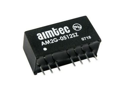 12V DC-DC Converter AM2G-0512SZ: Specifications, Datasheet, Applications and Features6/3/2024 684
A DC-DC converter is an essential electronic device to convert a direct current (DC) source from one voltage level to another. These converters are widely employed in various applications, including portable electronic devices, automotive systems, and renewable energy installations.
Read More >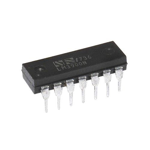 What is LM3900 Quadruple Norton Operational Amplifier?5/30/2024 1376
The LM3900 consists of four independent dual-input internally compensated amplifiers. These amplifiers are specifically designed to operate on a single power supply voltage and provide a large output voltage swing. They utilize current mirrors to achieve in-phase input functionality. Applications include AC amplifiers, RC active filters, low-frequency triangle waves, square wave, and pulse waveform generation circuits, tachometers, and low-speed, high-voltage digital logic gates.
Read More > Exploring the MMBT3906 Transistor: A Comprehensive Guide5/24/2024 986
The goal of the Taiwan Semiconductor MMBT3906 PNP Bipolar Transistor is to provide a high surge current capability with minimal power loss. This transistor is perfect for automated installation and has high efficiency.
Read More >
SUPPORT
ABOUT BITFOIC
QUICK LINKS
Connect with us
Tel: 86-755-23606554
E-mail: [email protected]
Address: Room A29, 24 / F, Hoi Tak Wai, Prince Edward industrial building, 706 Prince Edward Road East, San Po Kong, Kowloon,Hongkong
Mon-Fri: 09.30 AM - 18.30 PM


