


BD139 Bipolar Transistor Basics: Pinout, CAD Model, circuits, Features and Application
Introduction
The widely used NPN transistor BD139 is used in a wide range of electronic circuits. Because of its low price and high collector current, it is the perfect transistor for both commercial and educational electronic projects. Its ability to drive loads up to 1.5A is a useful feature that allows you to drive a variety of high-current components, including high-power LEDs, high-current relays, motors, and more. Because of the high collector-emitter and collector base voltages, it can easily work in electronic circuits with operating voltages as low as 80 volts. The collector dissipation is 12.5W which is also ideal to use in audio amplifier circuits. The saturation voltage of the transistor is just 0.5V.
Ⅰ What is BD139?
The BD139 is a bipolar medium power NPN transistor (BJT) in a TO-126 package designed for audio amplifiers and drivers utilizing complementary circuits. Since BD139 is an NPN transistor, the emitter, and collector are in a PN junction or open circuit (reverse bias). Also, when you ground a pin and receive a signal, the pin becomes forward-biased (closed).
Gain values for the BD139 range from 40 to 160, (the gain value of any transistor helps determine its amplification capabilities). The maximum current that can pass through the collector pin is 1.5A, so if you are using a BD139 transistor, make sure the load must be less than 1.5A. For the BD139 transistor to operate in a forward-biased state, we must apply a current at its base, and this base current must be greater than 1/10 of its collector current, moreover, make sure that at its base-emitter pin Apply 5V. Once it is running in forward bias, we can draw a maximum of 1.5A between its collector and emitter. If the maximum current (i.e. 1.5A) flows through the transistor then we can say it is in a saturation region. Usually, we can apply a maximum of 80V between the Collector & Base and when we remove the base current the transistor becomes completely off, this condition is called a cutoff region.
Ⅱ BD139 Pinout
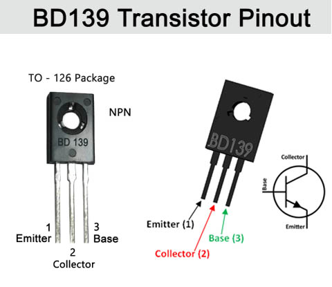
Figure1-bd139 pinout
Ⅲ BD139 Pinout Configuration
|
Pin Number |
Pin Name |
Description |
|
1 |
Emitter |
Current Drains out through emitter, normally connected to ground |
|
2 |
Collector |
Current flows in through the collector, normally connected to load |
|
3 |
Base |
Controls the biasing of the transistor, Used to turn ON or OFF the transistor. |
Ⅳ Features / technical specifications:
- Package Type: TO-126
- Transistor Type: NPN
- Max Collector Current(IC): 5A
- Max Collector-Emitter Voltage (VCE): 80V
- Max Collector-Base Voltage (VCB): 80V
- Max Emitter-Base Voltage (VEBO): 5V
- Max Collector Dissipation (Pc): 5 Watt
- Max Transition Frequency (ft): 190 MHz
- Minimum & Maximum DC Current Gain (hFE): 25 – 250
- Max Storage & Operating temperature Should Be: -55 to +150 Centigrade
Ⅴ BD139 transistor Equivalent
- The transistor equivalent for BD139 transistor is BD169, BD179, BD230, MJE244, or MJE722.
- Each one in the equivalent list is the perfect equivalent for the BD139 transistor.
- Most of the electrical specifications and technical specifications of all of the transistors are the same.
Ⅵ BD139 vs BD140 vs MJE242 vs BD379
|
|
BD139 |
BD140 (PNP) |
MJE242 |
BD379 |
|
Collector to base voltage (VCB) |
80V |
-80V |
80V |
100V |
|
Collector to emitter voltage (VCE) |
80V |
-80V |
80V |
80V |
|
Emitter to base voltage (VEB) |
5V |
-5V |
7V |
5V |
|
Collector current (IC) |
1.5A |
1.5A |
8A |
2A |
|
Power dissipation |
12.5W |
12.5W |
15W |
25W |
|
Junction temperature (TJ) |
150°C |
150°C |
150°C |
150°C |
|
Transition frequency (FT) |
50MHZ |
160MHZ |
40MHZ |
50MHZ |
|
Noise (N) |
——– |
——- |
——- |
——— |
|
Gain (hFE) |
25 to 250hFE |
25 to 250hFE |
25 to 250hFE |
30 to 250hFE |
|
Package |
TO-126 TO-225 |
TO-126 |
TO-126 |
TO-126 |
Ⅶ BD139 VS BD140
BD139 and BD140 are complementary NPN and PNP bipolar junction transistors (BJTs) commonly used in amplification and switching applications. They are often used in pairs to create a push-pull amplifier circuit.
The BD139 and BD140 have similar specifications but differ in their polarity. The BD139 is an NPN BJT, while the BD140 is a PNP BJT. They both have a maximum collector current rating of 1.5A, a maximum collector-emitter voltage rating of 80V, and a maximum power dissipation rating of 12.5W.
One major difference between the two is their hFE, or current gain. The hFE of BD139 ranges from 25 to 250, while the hFE of BD140 ranges from 40 to 250. This means that BD140 may have a slightly higher gain compared to BD139.
Another difference is their polarity, which affects how they are used in a circuit. NPN transistors like BD139 are used for switching and amplification of positive voltages, while PNP transistors like BD140 are used for switching and amplification of negative voltages.
Overall, the choice between BD139 and BD140 depends on the specific requirements of the circuit and the polarity of the voltages involved.
- RF amplifier circuit
- Switching circuits
- Amplifier circuits
- Audio amplifier circuits
- Load driver circuits
- Arduino circuit applications
Ⅸ BD139 package
- The BD139 transistor had TO-126 and TO-225 packages
- It is a rectangular-shaped transistor package with a hole in the middle portion.
- The hole at the middle portion supports the transistor to mount it with the board or with the heat sink.
- The plastic-epoxy material usage will make the transistor more temperature resistant and compatible
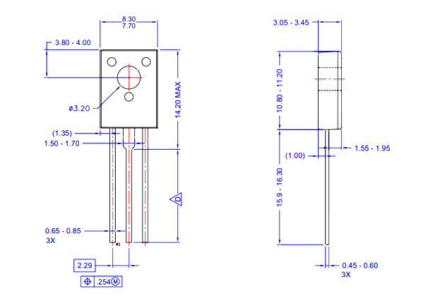
Figure2-TO-225
Ⅹ How to Safely Long Run in a Circuit:
Avoid operating this transistor from voltages higher than 80V, limit load current to 1.5A or 1500mA, and use an appropriate heat sink when using it in circuits or electrical projects to ensure its safety. Use a suitable base resistor as well to supply the necessary base current. Avoid exposing this transistor to temperatures below -55 °C and above +150 °C as they are below its minimum and maximum survival temperature, respectively.
Ⅺ Where to use BD136 Transistor
Being a Medium Power NPN Transistor with a collector current of 1.5A this transistor can be used to control (On/Off) bigger loads that consume less than 1.5A. It also has a very less saturation voltage (Base Emitter Voltage VBE) of only 5V, which makes it easy to use this IC in digital electronics which has an operating voltage of 5V.
Another peculiar fact about this transistor is that it comes in a plastic package, while most medium power transistors are available only in a metal can package. This reduces the cost of the Transistor and also since the package is not conductive it will not be affected by other noise in the circuit. Due to this feature, this transistor is widely used in amplifier applications.
So if you are looking for a medium-power NPN transistor in Plastic package then this Transistor might be the right choice for you.
Ⅻ BD139 switch circuit
The basic model switch circuit employing the BD139 transistor is shown in the image. The circuit uses two resistors to drive a transistor and LEDs. The transistor's base resistor produces a voltage that triggers the BD139 transistor when the switch shuts. The LED then begins to illuminate as the trigger pulse reaches it.
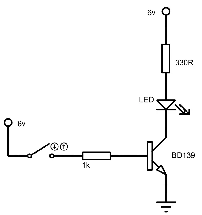
Figure3-BD139 switch circuit
XIII BD139 amplifier circuit
A miniature amplifier circuit using a BD139 transistor is shown in the figure. The two-stage transistors 2n3904 and BD139 make up the amplifier circuit. In terms of technical details, the transistors are similar. Because of their similar emitter arrangement, the transistors bypass the Q1 transistor when the input signal reaches the input capacitor. The signal is boosted by the Q1 transistor before moving on to the Q2 transistor. Second-stage amplification is performed by the Q2 transistor BD139 before it moves on to the output.
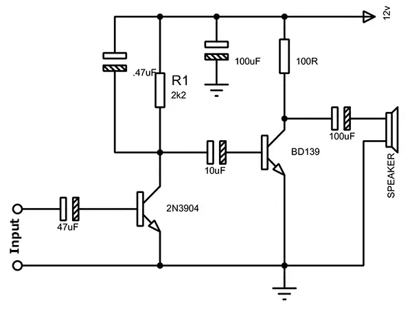
Figure4-BD139 amplifier circuit
XIV BD139 Arduino
The BD139 transistor, which was used in projects for speed control, is depicted in the Arduino project in the picture. As we can see from the circuit, the BD139 is linked to the PMW terminal and is used to regulate the cooler's speed. The speed of the cooler is controlled by a pulse generated by the Arduino board and the BD139 transistor.
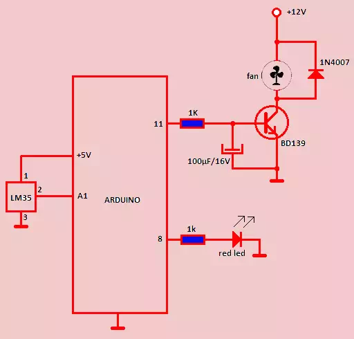
Figure5-BD139 Arduino
XV BD139 Datasheet
 How to resolve the WiFi and ADC2 Sharing Dilemma?4/19/2024 10
ESP32-CAM can be used in various Internet of Things situations and is suitable for home smart devices, industrial wireless control, wireless Monitoring, QR wireless identification, wireless positioning system signals, and other IoT applications are ideal solutions for IoT applications.
Read More > ESP32-CAM Pinout Explanation and How to Use?4/18/2024 17
ESP32-CAM is a development board with an ESP32-S chip, an OV2640 camera, a microSD card slot, and several GPIOs for connecting peripherals. ESP32-CAM is a small-sized camera module. The module can work independently as the smallest system, with a size of only 27*40.5*4.5mm.
Read More > Stand-Alone Linear Li-Ion / Li-Polymer Charge Management Controller MCP738334/9/2024 51
The MCP73833/4 is a highly advanced linear charge management controller for use in space-limited, cost sensitive applications. Both a 10-lead, MSOP and a 10-lead, DFN packaging measuring 3 mm by 3 mm are offered for the MCP73833/4. In addition to its tiny size, the MCP73833/4 is perfect for portable applications because it requires a few additional components.
Read More >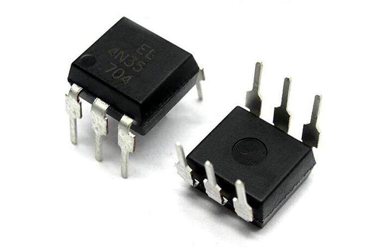 Optocoupler IC 4N35: Pinout, Datasheet, Features and Applications3/26/2024 77
In the realm of electronics, where connectivity and isolation are paramount, the 4N35 optocoupler IC stands as a beacon of reliability and versatility. This small yet mighty device plays a crucial role in ensuring signal integrity and safety across a wide range of applications. In this article, we delve into the intricacies of the 4N35 optocoupler IC, exploring its datasheet, pinout, circuit diagram, and diverse uses.
Read More > UA741CP datasheet ,Specification, Features and Application3/21/2024 80
The UA741CP is a general-purpose operational amplifier in an 8-pin DIP package. The high common-mode input voltage range and lack of latch-up make the amplifier ideal for voltage follower applications.
Read More >
SUPPORT
ABOUT BITFOIC
QUICK LINKS
Connect with us
Tel: 86-755-23606554
E-mail: contact@bitfoic.com
Address: Room A29, 24 / F, Hoi Tak Wai, Prince Edward industrial building, 706 Prince Edward Road East, San Po Kong, Kowloon,Hongkong
Mon-Fri: 09.30 AM - 18.30 PM


